S15: Protocol Interface: I2C - CAN Bridge
Contents
- 1 Serial Protocol Convertor
- 2 Abstract
- 3 Objectives & Introduction
- 4 Team Members & Responsibilities
- 5 Schedule
- 6 Parts List & Cost
- 7 Hardware Design
- 8 Hardware Interface
- 9 Software Design
- 10 Implementation
- 11 Testing & Technical Challenges
- 12 Conclusion
- 13 Project Video
- 14 Project Source Code
- 15 References
Serial Protocol Convertor
AbstractThis project is aimed at developing a device that can act as an interface between I2C bus and CAN bus. This device "Protocol Interface: I2C - CAN Birdge" can receive the data over CAN bus and can give it to a device connected on an I2C bus. The data is stored using a mailbox concept meaning message with different CAN ID is stored in different mailboxes. The mailboxes can be configured for a specific CAN ID, CAN ID with Mask Bits and different sizes.
Objectives & IntroductionBasically, this device will convert the incoming data from one protocol to the other desired protocol. Considering the problems faced in an industry, the main goal of this project is to enable the designers to use a controller, that supports any serial protocol, to the system using CAN bus. For designing a protocol converter, there are some aspects such as speed synchronization and bi-directional communication, which are necessary to make this device useful. A practical example would be connecting an I2C device to the CAN system. Since the I2C protocol consists of a master - slave approach, it is not possible to control the I2C master by I2C slave. In this project, these conditions are handled using hardware interrupts. Also speed synchronization is a crucial aspect, as every protocol supports different data speed. The concept of Queues and Mailboxes is used to handle the speed limitations. FreeRTOS is used for designing the software of this system. |
Team Members & Responsibilities
| S.R. | Team Member's Name | Tasks |
|---|---|---|
| 1 | Ishan Bhavsar |
|
| 2 | Tej Kogekar | |
| 3 | Rutwik Kulkarni |
|
| 4 | Mitesh Sanghvi |
Schedule
| S.R. | Start Date | End Date | Task | Status | Actual Completion Date |
|---|---|---|---|---|---|
| 1 | 03/08/2015 | 03/14/2015 | Develop driver for interrupt based I2C acting as a Slave Device | Completed | 03/14/2015 |
| 2 | 03/15/2015 | 03/21/2015 | Exploring CAN API and building CAN bus for communication | Completed | 03/21/2015 |
| 3 | 03/22/2015 | 03/28/2015 | Study and Design mailbox system for CAN messages | Completed | 03/28/2015 |
| 4 | 03/29/2015 | 04/04/2015 | Develop program for configuring the Protocol Interface by I2C Master | Completed | 04/04/2015 |
| 5 | 04/05/2015 | 04/11/2015 | Create task for storing CAN messages in mailboxes | Completed | 04/11/2015 |
| 6 | 04/12/2015 | 04/18/2015 | Create task for giving interrupt to I2C Master | Completed | 04/18/2015 |
| 7 | 04/19/2015 | 04/25/2015 | Create task for sending message on CAN recieved from I2C Master | Completed | 04/25/2015 |
| 8 | 04/26/2015 | 05/02/2015 | Design of Status Register for Protocol Interface | Completed | 05/02/2015 |
| 9 | 05/03/2015 | 05/09/2015 | Finalizing appropriate addresses for all registers | Completed | 05/09/2015 |
| 10 | 05/10/2015 | 05/16/2015 | Testing of Protocol Interface for various conditions | Completed | 05/12/2015 |
| 11 | 05/17/2015 | 05/23/2015 | Adding a feature of Bit-Masked CAN IDs | Completed | 05/22/2015 |
Parts List & Cost
| S.R. | Description | Manufacturer | Part Number | Qty | Cost |
|---|---|---|---|---|---|
| 1 | SJOne Board | - | - | 1 | $80.00 |
| 2 | Ultrasonic Sensor (Optional) | Parallax | 28015 | 1 | $23.00 |
| 3 | CAN Transceiver (Free Samples) | Microchip | MCP2551 | 1 | $0.00 |
| 4 | Linear Voltage Regulator (Free Sample) | LT | LT1083-5 | 1 | $0.00 |
| Total | $103.00 | ||||
Hardware Design
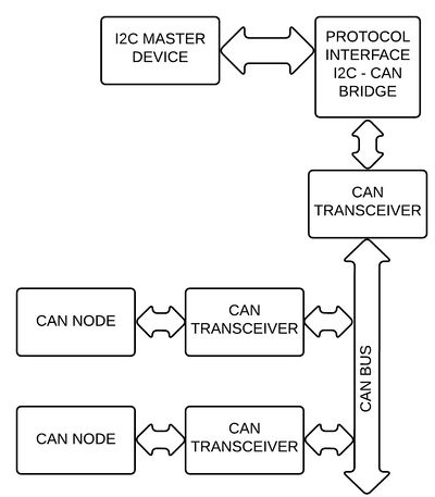
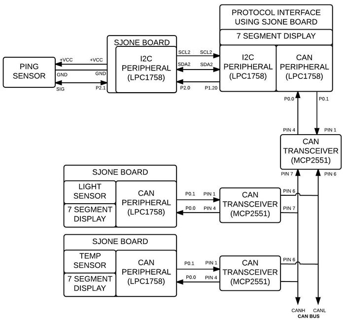
This project is used as an interface for an I2C controller to communicate over the CAN bus. The I2C controller should act as an I2C master and the Protocol Interface device will act as an I2C slave device. Since the communication from the I2C slave to the I2C master is not possible, external GPIO interrupts are used. The Protocol Interface has an inbuilt CAN peripheral to communicate over the CAN bus. The I2C master is supposed to configure the mailboxes of the interface for the particular CAN ID’s. These mailboxes are used to store the CAN messages received by the Protocol Interface over the CAN bus. Whenever a message is received by the CAN peripheral, it is stored in the respective mailbox. Once the number of Data Frames stored in any mailbox reached the limit (configured by I2C Master), an interrupt is given. The Protocol Interface uses SJOne development board for the communication that supports both I2C and CAN protocols. The write and read address of the Protocol Interface is 0x50 and 0x51 respectively, which are used by the I2C master for the communication.
Hardware Interface
I2C Bus
The following shows the I2C bus protocol:
- Data transfer is initiated by master device only, when the bus is not busy.
- Data is clocked in; when the clock line (SCL) is HIGH, the state data line (SDA) determines value of the incoming bit. The START or STOP condition are given by changing state of SDA line when SCL line is high.
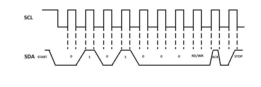
The states of the diagram are described in detail below:
- IDLE state: both data and clock lines remain HIGH.
- START condition: a HIGH to LOW transition of the SDA line when the SCL line is HIGH. All transactions must be preceded by a START condition.
- STOP condition: a LOW to HIGH transition of the SDA line while the SCL is HIGH. All transactions must be terminated by a STOP condition.
- Data transfer: the data transfer is preceded by a START condition. The state of data line during HIGH period of the SCL represents data bits. The state of data line is changed during the LOW period of the SCL. The data transfer is terminated with a STOP condition. The master device controls the data flow.
- Acknowledgement: After reception of each data byte, the receiver sends the acknowledgement bit. During master write mode, the ACK bit sent by slave signifies that it can accommodate more data. If the slave sends NACK then it cannot accommodate any more data. To acknowledge the slave has to pull down the SDA line during the acknowledge clock pulse during the HIGH period of SCL.
CAN Bus
Controller Area Network (CAN) is a communication protocol which is developed by Bosch. It can be summarized as follows:
- The physical layer of the protocol uses twisted pair wire for transmission and reception of differential signal.
- A deterministic bus which uses non destructive bit wise arbitration.
- It uses small messages (around 8 bytes) protected by checksum for data integrity.
- Instead of explicit addressing, it uses 11 bit or 29 bit identifier which controls its priority on the bus.
- A sophisticated error handling mechanism, where error in message can be handled by retransmission of message.
- Effective mechanism to isolate faults and removing faulty nodes from the bus.
- Because of reliability, noise immunity it is extensively used in automotive industry for effective and efficient communication between different types of controllers.
- The speeds supported by CAN bus are 100K, 250K, 500K, 1MBits per second.
CAN Transceiver
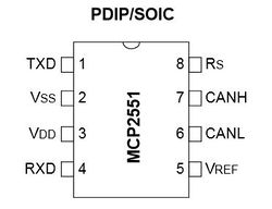
The microprocessor’s inbuilt CAN peripheral cannot directly communicate over the CAN bus. It needs a CAN transceiver to be connected between peripheral and bus. The main two task of CAN transceiver are:
- Receiving: It adapts signal levels from the bus, to levels that the CAN Controller expects. It generally comes with a protective circuitry that protects the processor’s internal CAN peripheral.
- Sending: It converts the transmit-bit signal received from the microcontroller’s internal CAN peripheral into a signal that needs to be sent onto the CAN bus.
- Supports 1Mbps speed of operation.
- Sutaible for 12V and 24V systems.
- Externally-controlled slope for reduced RFI systems.
- Power on reset and voltage brown out protection.
- Low current standby operation.
- Protection against short circuit protection in case of positive or negative battery voltage. It also has thermal shutdown protection, protection against high voltage transients.
Software Design
Configure MailboxThe flowchart for configuring mailboxes is as shown in Figure2. The algorithm is as follows:
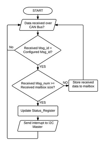
CAN to MailboxThe flowchart for storing data received over CAN to mailbox is as shown in Figure3. The algorithm is as follows:
|
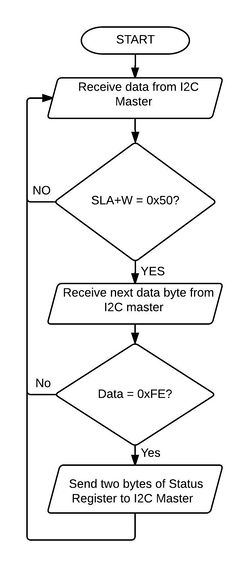
Read Status RegisterThe flowchart for reading Status Register of Protocol Interface is as shown in Figure4. The algorithm is as follows:
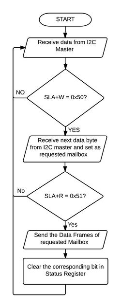
Read Mailbox DataThe flowchart for reading mailbox data is as shown in Figure5. The algorithm is as follows:
|
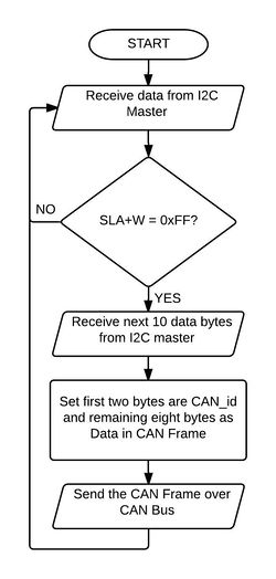
Send Data over CANThe flowchart for sending data from I2C Master to CAN is as shown in Figure6. The algorithm is as follows:
|
Implementation
The steps involved in implementation of this project are as follows:
- During boot-up process of Protocol Interface, I2C and CAN drivers are initialized.
- The device is ready to accept messages from I2C Master to be sent over the CAN bus. The data frame is as follows:
- The I2C Master write data to Configuration Registers of respective Mailbox. The data frame is as follows:
- According to the Configuration Registers, the mailboxes are configured for specific CAN_id, size and optional Mask_id.
- The device will continuously keep on accepting messages from CAN bus. For every message received, the software will check whether the received CAN_id matches with the configured mailbox CAN_id. If the id matches, then the Data Frame i.e. CAN_id and 8-bytes of Data is stored in the particular mailbox.
- For all the received messages, if a particular mailbox is configured with Mask_id, then it will also check the received CAN_id to match with the masked CAN_id.
- Once the message is saved in the mailbox, it will check whether the number of frames stored in a mailbox exceeds the configured size for that mailbox. If it exceeds, then device will give an external GPIO interrupt to I2C Master.
- On receiving an interrupt, I2C Master will initiate read transaction to read the Status Register. The data frame is as follows:
- Looking at the bits set in the Status Register, I2C Master will decide to read the data from any one mailbox at a time.
- I2C Master will initiate read transaction for one mailbox and device will send the data frames of requested mailbox. The data frame is as follows:
Testing & Technical Challenges
Describe the challenges of your project. What advise would you give yourself or someone else if your project can be started from scratch again? Make a smooth transition to testing section and described what it took to test your project.
Include sub-sections that list out a problem and solution, such as:
Issues Faced
I2C Slave to I2C Master Communication
Once I2C Master configures the mailbox for a specific size, it will keep a track of the number of data frames present in a particular mailbox. But, once the number of frames exceeds the configured size, the Protocol Interface being an I2C Slave, cannot initiate a transaction and ask I2C Master to read the data. So, whenever the number of data frames for any mailbox exceeds the configured size, it will send an interrupt to I2C Master informing that at least one of the mailbox is exceeding the number of data frames. In response to this interrupt, I2C Master can initiate a read transaction and read the data from the mailbox.
Which Mailbox is FULL?
The size configured for each mailbox can be different. The device will send an interrupt whenever the number of messages in any mailbox exceeds the configured size. But, by getting an interrupt, I2C Master does not know that which mailbox is full. So it needs to initiate a read transaction for maximum number of data bytes. But, in doing that, the device (acting as an I2C Slave) can not send NACK to I2C Master saying that the data is over. So we introduced a concept of a Status Register. Status Register clearly defines that which mailbox is full. Adding this concept also gives an added feature of priority. When I2C Master reads the Status Register, it gets information about all the mailboxes that are full. So, depending on the priority, an I2C Master can decide on which mailbox's data to be read first.
Multiple Interrupts for Same Mailbox
We had faced a situation where the I2C slave device was giving multiple interrupts for the same mailbox. This issue was solved by restricting the interrupt send function by reading the status bit before sending an interrupt.
Conclusion
Conclude your project here. You can recap your testing and problems. You should address the "so what" part here to indicate what you ultimately learnt from this project. How has this project increased your knowledge?
Project Video
Upload a video of your project and post the link here.
Project Source Code
References
- LPC_USER_MANUAL
- Ultrasonic Sensor
- CAN Transceiver
- Linear Voltage Regulator
- Socialledge Embedded Systems Wiki
- Preetpal Kang, Lecture notes of CMPE 243, Computer Engineering, Charles W. Davidson College of Engineering, San Jose State University, Aug-Dec 2014.
- en.wikipedia.org/
