S15: Protocol Interface: I2C - CAN Bridge
Contents
- 1 Serial Protocol Convertor
- 2 Abstract
- 3 Objectives & Introduction
- 4 Team Members & Responsibilities
- 5 Schedule
- 6 Parts List & Cost
- 7 Design & Implementation
- 8 Hardware Design
- 9 Hardware Interface
- 10 Software Design
- 11 Implementation
- 12 Testing & Technical Challenges
- 13 Conclusion
- 14 Project Video
- 15 Project Source Code
- 16 References
Serial Protocol Convertor
Abstract
This project is aimed at developing a device, which is able to convert the incoming data from one protocol to another (I2C, UART, SPI, CAN). In a system operating over a CAN architecture, there is a need of an inbuilt CAN peripheral interface in every controller. Because of hardware limitations, many controllers do not support the CAN peripherals; therefore they are restricted to communicate over the limited number of protocols. This device provides a flexibility to the designers so that they can choose any communication protocol at the input, and convert the data to the desired protocol.
Objectives & Introduction
Basically, this device will convert the incoming data from one protocol to the other desired protocol. Considering the problems faced in an industry, the main goal of this project is to enable the designers to use a controller, that supports any serial protocol, to the system using CAN bus. For designing a protocol converter, there are some aspects such as speed synchronization and bi-directional communication, which are necessary to make this device useful. A practical example would be connecting an I2C device to the CAN system. Since the I2C protocol consists of a master - slave approach, it is not possible to control the I2C master by I2C slave. In this project, these conditions are handled using hardware interrupts. Also speed synchronization is a crucial aspect, as every protocol supports different data speed. The concept of Queues and Mailboxes is used to handle the speed limitations. FreeRTOS is used for designing the software of this system.
Team Members & Responsibilities
| S.R. | Team Member's Name | Tasks |
|---|---|---|
| 1 | Ishan Bhavsar |
|
| 2 | Tej Kogekar | |
| 3 | Rutwik Kulkarni |
|
| 4 | Mitesh Sanghvi |
Schedule
| S.R. | Start Date | End Date | Task | Status | Actual Completion Date |
|---|---|---|---|---|---|
| 1 | 03/08/2015 | 03/14/2015 | Develop driver for interrupt based I2C acting as a Slave Device | Completed | 03/14/2015 |
| 2 | 03/15/2015 | 03/21/2015 | Exploring CAN API and building CAN bus for communication | Completed | 03/21/2015 |
| 3 | 03/22/2015 | 03/28/2015 | Study and Design mailbox system for CAN messages | Completed | 03/28/2015 |
| 4 | 03/29/2015 | 04/04/2015 | Develop program for configuring the Protocol Interface by I2C Master | Completed | 04/04/2015 |
| 5 | 04/05/2015 | 04/11/2015 | Create task for storing CAN messages in mailboxes | Completed | 04/11/2015 |
| 6 | 04/12/2015 | 04/18/2015 | Create task for giving interrupt to I2C Master | Completed | 04/18/2015 |
| 7 | 04/19/2015 | 04/25/2015 | Create task for sending message on CAN recieved from I2C Master | Completed | 04/25/2015 |
| 8 | 04/26/2015 | 05/02/2015 | Design of Status Register for Protocol Interface | Completed | 05/02/2015 |
| 9 | 05/03/2015 | 05/09/2015 | Finalizing appropriate addresses for all registers | Completed | 05/09/2015 |
| 10 | 05/10/2015 | 05/16/2015 | Testing of Protocol Interface for various conditions | Completed | 05/12/2015 |
| 11 | 05/17/2015 | 05/23/2015 | Adding a feature of Bit-Masked CAN IDs | Completed | 05/22/2015 |
Parts List & Cost
| S.R. | Description | Manufacturer | Part Number | Qty | Cost |
|---|---|---|---|---|---|
| 1 | SJOne Board | - | - | 1 | $80.00 |
| 2 | Ultrasonic Sensor (Optional) | Parallax | 28015 | 1 | $23.00 |
| 3 | CAN Transceiver (Free Samples) | Microchip | MCP2551 | 1 | $0.00 |
| 4 | Linear Voltage Regulator (Free Sample) | LT | LT1083-5 | 1 | $0.00 |
| Total | $103.00 | ||||
Design & Implementation
The design section can go over your hardware and software design. Organize this section using sub-sections that go over your design and implementation.
Hardware Design
This project is used as an interface for an I2C controller to communicate over the CAN bus. The I2C controller should act as an I2C master and the Protocol Interface device will act as an I2C slave device. Since the communication from the I2C slave to the I2C master is not possible, external GPIO interrupts are used. The Protocol Interface has an inbuilt CAN peripheral to communicate over the CAN bus. The I2C master is supposed to configure the mailboxes of the interface for the particular CAN ID’s. These mailboxes are used to store the CAN messages received by the Protocol Interface over the CAN bus. Whenever a message is received by the CAN peripheral, it is stored in the respective mailbox. Once the number of Data Frames stored in any mailbox reached the limit (configured by I2C Master), an interrupt is given. The Protocol Interface uses SJOne development board for the communication that supports both I2C and CAN protocols. The write and read address of the Protocol Interface is 0x50 and 0x51 respectively, which are used by the I2C master for the communication.
Hardware Interface
In this section, you can describe how your hardware communicates, such as which BUSes used. You can discuss your driver implementation here, such that the Software Design section is isolated to talk about high level workings rather than inner working of your project.
Software Design
Configure MailboxThe flowchart for configuring mailboxes is as shown in Figurex. The algorithm is as follows:
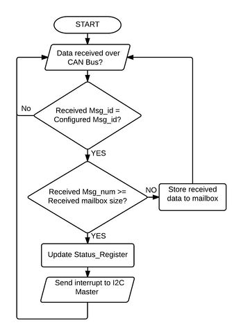
CAN to MailboxThe flowchart for storing data received over CAN to mailbox is as shown in Figurex. The algorithm is as follows:
|
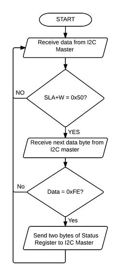
Read Status RegisterThe flowchart for reading Status Register of Protocol Interface is as shown in Figurex. The algorithm is as follows:
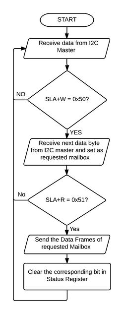
Read Mailbox DataThe flowchart for reading mailbox data is as shown in Figurex. The algorithm is as follows:
|
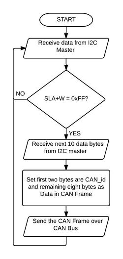
Send Data over CANThe flowchart for sending data from I2C Master to CAN is as shown in Figurex. The algorithm is as follows:
|
Implementation
The steps involved in implementation of this project are as follows:
- During boot-up process of Protocol Interface, I2C and CAN drivers are initialized.
- The device is ready to accept messages from I2C Master to be sent over the CAN bus. The data frame is as follows:
- The I2C Master write data to Configuration Registers of respective Mailbox. The data frame is as follows:
- According to the Configuration Registers, the mailboxes are configured for specific CAN_id, size and optional Mask_id.
- The device will continuously keep on accepting messages from CAN bus. For every message received, the software will check whether the received CAN_id matches with the configured mailbox CAN_id. If the id matches, then the Data Frame i.e. CAN_id and 8-bytes of Data is stored in the particular mailbox.
- For all the received messages, if a particular mailbox is configured with Mask_id, then it will also check the received CAN_id to match with the masked CAN_id.
- Once the message is saved in the mailbox, it will check whether the number of frames stored in a mailbox exceeds the configured size for that mailbox. If it exceeds, then device will give an external GPIO interrupt to I2C Master.
- On receiving an interrupt, I2C Master will initiate read transaction to read the Status Register. The data frame is as follows:
- Looking at the bits set in the Status Register, I2C Master will decide to read the data from any one mailbox at a time.
- I2C Master will initiate read transaction for one mailbox and device will send the data frames of requested mailbox. The data frame is as follows:
Testing & Technical Challenges
Describe the challenges of your project. What advise would you give yourself or someone else if your project can be started from scratch again? Make a smooth transition to testing section and described what it took to test your project.
Include sub-sections that list out a problem and solution, such as:
My Issue #1
Discuss the issue and resolution.
Conclusion
Conclude your project here. You can recap your testing and problems. You should address the "so what" part here to indicate what you ultimately learnt from this project. How has this project increased your knowledge?
Project Video
Upload a video of your project and post the link here.
Project Source Code
References
Acknowledgement
Any acknowledgement that you may wish to provide can be included here.
References Used
- LPC_USER_MANUAL
- Ultrasonic Sensor
- GLCD with Touchscreen
- CAN Transceiver
- Linear Voltage Regulator
- Socialledge Embedded Systems Wiki
- Preetpal Kang, Lecture notes of CMPE 243, Computer Engineering, Charles W. Davidson College of Engineering, San Jose State University, Aug-Dec 2014.
- en.wikipedia.org/


