Difference between revisions of "S15: Remote Learner"
(→Hardware Design) |
(→Hardware Interface) |
||
| Line 250: | Line 250: | ||
[[File:NEC_IR.JPG|500px]] | [[File:NEC_IR.JPG|500px]] | ||
<br>In the above image is a capture of a NEC IR transmission using an oscilloscope. | <br>In the above image is a capture of a NEC IR transmission using an oscilloscope. | ||
| + | |||
| + | <br><b>IR Receiver to Capture Pin:</b><br> | ||
| + | The IR receiver outputs a logic one (high, 3.3v) signal when idle. When active, the signal drops to a logic zero (low, 0v). Therefore, the signal is active low, which may actually be inverted relative to the transmitted signal. The images below show two examples of transmitted signals and receiver output. | ||
| + | |||
| + | [[File:S15_244_RemoteLearner_IR_Receiver_Waveform1.png|400px|centre|thumb|IR receiver output given typical pulse input signal]] | ||
| + | [[File:S15_244_RemoteLearner_IR_Receiver_Waveform2.png|400px|centre|thumb|IR receiver output given pulse burst input signal]] | ||
| + | |||
| + | These images are from the IR receiver data sheet included in the development package of the SJOne board. However, you can find it on Vishay's website as well. This signal is physically connected to one of the capture pins on the LPC microcontroller. In our example, the board is designed to take this input on P1[18] using CAP1[0]. | ||
| + | |||
| + | The capture feature is associated with one of the boards timers. In our case, this is timer 1 (hence CAP1). The [0] indicates port 0. Timer 1 is used by the development package, so it should already be started for us. All we need to do is configure the Capture Control Register to generate an input on both rising and falling edges. | ||
| + | |||
| + | When this interrupt occurs, we get a tick count. We don't need to know the time exactly, just the difference in times between captures. Since the IR receiver idles high, we know the first interrupt will be for a falling edge. We can perform the calculations according to this assumption. | ||
=== Software Design === | === Software Design === | ||
Revision as of 05:47, 23 May 2015
Contents
Grading Criteria
- How well is Software & Hardware Design described?
- How well can this report be used to reproduce this project?
- Code Quality
- Overall Report Quality:
- Software Block Diagrams
- Hardware Block Diagrams
- Schematic Quality
- Quality of technical challenges and solutions adopted.
Remote Learner
Abstract
The objective of this project was to create a remote learner using the SJOne board. The Remote Learner would have the ability to be controlled by an Android application using Bluetooth. The application would tell the SJOne board to learn a remote control using the IR sensor or transmit the remote command via IR LED..
Objectives & Introduction
Show list of your objectives. This section includes the high level details of your project. You can write about the various sensors or peripherals you used to get your project completed.
Team Members & Responsibilities
- Bailey Wu - Android App and BT I/F
- Yoni Klein - RX and IR Learning
- Tejeswar - IR Protocol
- Christopher Laurence - TX
Schedule
Remote Learner
| Week | Start Date | End Date | Task | Status | Actual Completion Date |
|---|---|---|---|---|---|
| 1-2 | 3/27/2015 | 4/10/2015 | Research about the basic of remote controller protocols | Completed | 3/10/15 |
| 3 | 4/10/2015 | 4/17/2015 | Research about transmit timing of the protocol and analyze the data with a oscilloscope
Research about receive timing of the protocol and analyze the data with a oscilloscope |
Completed | 4/17/2015 |
| 4 | 4/17/2015 | 4/24/2015 | Accurately decode IR signals from a remote control
Accurately transmit IR signals to a device |
Completed | 5/2/2015 |
| 5 | 4/24/2015 | 5/1/2015 | Interface BT module and establish communication with the Android phone
Decide on a communication protocol between phone and board. |
Planned | TBD |
| 6-7 | 5/1/2015 | 5/15/2015 | Research and add additional protocol support | Completed | 5/15/2015 |
| 8 | 5/15/2015 | 5/22/2015 | Final integration and testing. | Planned | TBD |
Android Application
| Week | Start Date | End Date | Task | Status | Actual Completion Date |
|---|---|---|---|---|---|
| 1 | 4/6/2015 | 4/13/2015 | Research about Android application development
Research about Bluetooth module implementation with SJOne board |
Completed | 4/10/2015 |
| 2 | 4/13/2015 | 4/20/2015 | Implement and design a basic Android application on Android Studio
Implement the Bluetooth module using UART |
Ongoing | TBD |
| 3 | 4/20/2015 | 4/27/2015 | Continue development of the Android application
Establish a connection between the SJOne board and Android application through Bluetooth |
Planned | TBD |
| 4 | 4/27/2015 | 5/4/2015 | Collaborate with team members to integrate the Android application and remote learner functions | Planned | TBD |
| 5 | 5/4/2015 | 5/11/2015 | Debug and troubleshoot any issues that may arise | Planned | TBD |
| 6 | 5/11/2015 | 5/18/2015 | Miscellaneous | Planned | TBD |
Parts List & Cost
Give a simple list of the cost of your project broken down by components. Do not write long stories here.
| Line Item# | Part Desciption | Vendor | Part Number | Qty | Cost ($) |
|---|---|---|---|---|---|
| 1 | 120 Resistor | Anchor Electronic | N/A | 10 | 1.00 |
| 2 | IR LED 1.5 V 40mA | Anchor Electronic | N/A | 4 | 1.00 |
Design & Implementation
The design section can go over your hardware and software design. Organize this section using sub-sections that go over your design and implementation.
Hardware Design
Discuss your hardware design here. Show detailed schematics, and the interface here.
|
Transmit IR LED:
|
File:IR LED Circuit.png IR LED circuit |
Receive IR LED:
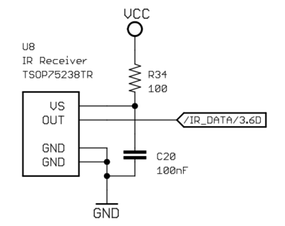
The IR receiver is already part of the SJOne board. On our revision 4 board, this is the TSOP75238TR IR Receiver Module by Vishay Semiconductors. Other revision boards may have a slightly different part, but the operation and concepts are the same.
The basic circuit is relatively simple. Along with power and ground, an output signal is connected to two different parts of the board.
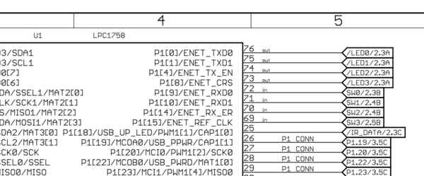
The first connection is made to P1[18] on the LPC controller. This GPIO pin will be configured to use the capture feature of the boards timer in order to "capture" the time a rising or falling signal event occurs. This pin is labeled as "IR_DATA" on the board schematic and the associated GPIO function is referred to as CAP1[0] in the user manual. The operation of the capture pin is described in the Hardware Interface section below.
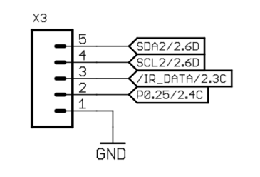
The second connection is to an external pin referenced in section 6D on page 3 of the board schematic. This is mainly used for debugging and validating captured data on an oscilloscope. Thanks Preet for adding this! Both of these connections are displayed in the images below.
Hardware Interface
In this section, you can describe how your hardware communicates, such as which BUSes used. You can discuss your driver implementation here, such that the Software Design section is isolated to talk about high level workings rather than inner working of your project.
PWM to IR LED:
The PWM was used to generate the 38 Khz by creating an instance of PWM class. Then using the predefined function of "pwm.set" to toggle the pin at a duty cycle of about 25% and after certain amount of time we set the duty cycle to 0. Below is the standard behavior for NEC IR protocol explaining the amount of time that the PWM pin needs to toggle and time required to be off.
| Protocol | On(µs) | Off(µs) | Total(µs) |
|---|---|---|---|
| Start | 9000 | 4500 | 13500 |
| 0 bit | 560 | 560 | 1120 |
| 1 bit | 560 | 1690 | 2250 |
| End | 560 | N/A | 560 |
500px
In the above image is a capture of a NEC IR transmission using an oscilloscope.
IR Receiver to Capture Pin:
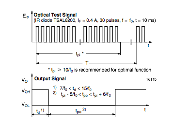
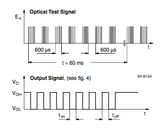
The IR receiver outputs a logic one (high, 3.3v) signal when idle. When active, the signal drops to a logic zero (low, 0v). Therefore, the signal is active low, which may actually be inverted relative to the transmitted signal. The images below show two examples of transmitted signals and receiver output.
These images are from the IR receiver data sheet included in the development package of the SJOne board. However, you can find it on Vishay's website as well. This signal is physically connected to one of the capture pins on the LPC microcontroller. In our example, the board is designed to take this input on P1[18] using CAP1[0].
The capture feature is associated with one of the boards timers. In our case, this is timer 1 (hence CAP1). The [0] indicates port 0. Timer 1 is used by the development package, so it should already be started for us. All we need to do is configure the Capture Control Register to generate an input on both rising and falling edges.
When this interrupt occurs, we get a tick count. We don't need to know the time exactly, just the difference in times between captures. Since the IR receiver idles high, we know the first interrupt will be for a falling edge. We can perform the calculations according to this assumption.
Software Design
Show your software design. For example, if you are designing an MP3 Player, show the tasks that you are using, and what they are doing at a high level. Do not show the details of the code. For example, do not show exact code, but you may show psuedocode and fragments of code. Keep in mind that you are showing DESIGN of your software, not the inner workings of it.
IR Transmit Task:
The IR transmit task will be signaled by the Bluetooth task. After being signal the task will attempt to read from a file using the Storage class. If the file doesn't exist it will send an error message to the Bluetooth task. If the file does exist then the task will read all the timing values into an array. The task will then enter a PortCritical area and transmit the IR signal by turning on and off the PWM pin. Once it is finished the IR Transmit task will signal the Bluetooth task with a successful message.
Implementation
This section includes implementation, but again, not the details, just the high level. For example, you can list the steps it takes to communicate over a sensor, or the steps needed to write a page of memory onto SPI Flash. You can include sub-sections for each of your component implementation.
Testing & Technical Challenges
Describe the challenges of your project. What advise would you give yourself or someone else if your project can be started from scratch again? Make a smooth transition to testing section and described what it took to test your project.
Include sub-sections that list out a problem and solution, such as:
IR Transmit Issue #1
PROBLEM:
IR transmission signal was not being received by IR receiver.
RESOLUTION:
Used Oscilloscope to discover that PWM instance set to 38,000 Hz did not produce a 38 kHz. Had to adjust the value to about 3205 Hz to get a PWM signal that was about 38Khz.
FUTURE RECOMMENDATIONS:
Examine PWM code and determine if there is a way to enter the fequency in Khz.
IR Transmit Issue #2
PROBLEM:
Putting IR transmission signal in task was causing IR signal not to be received because task was being interrupted.
RESOLUTION:
Placed time sensitive code in a Port Critical section to prevent that section of code being interrupted.
Conclusion
Conclude your project here. You can recap your testing and problems. You should address the "so what" part here to indicate what you ultimately learnt from this project. How has this project increased your knowledge?
Project Video
Upload a video of your project and post the link here.
Project Source Code
References
Acknowledgement
Any acknowledgement that you may wish to provide can be included here.
References Used
List any references used in project.
Appendix
You can list the references you used.
