Difference between revisions of "S14: Hyperintelligent NFC Locker of the Future"
Proj user18 (talk | contribs) (→Locking System) |
Proj user18 (talk | contribs) (→NFC Software Design) |
||
| Line 221: | Line 221: | ||
Packets from the PN532 to the host controller generally do not include the Preamble byte. | Packets from the PN532 to the host controller generally do not include the Preamble byte. | ||
| + | |||
| + | Commands sent form the host controller to the PN532 follow a certain pattern. First the host controller sends a packet to the PN532. Then PN532 then sends an interrupt to the host controller it to receive an acknowledgement (or non acknowledgement) from the PN532. This indicates that the PN532 has registered the send command as valid (or invalid). The PN532 then interrupts the host controller again much later after the command has finished and the host controller can fetch the result for the command. This design uses the interrupt pin, but another system can instead constantly poll the status register of the PN532 to see when it is ready. | ||
'''Normal Operation of SPI interface:''' | '''Normal Operation of SPI interface:''' | ||
[[File:CmpE146 S14 NFCLocker NFCSPIFRAME.jpg|400px|none]] | [[File:CmpE146 S14 NFCLocker NFCSPIFRAME.jpg|400px|none]] | ||
| + | |||
When the PN532 is turned on (or after the reset pin is inactivated), the PN532 goes into LowVBat mode. When ever the PN532 is in a low power consumption state, it requires some time before the packet can be sent from the host to the PN532. This can be done in two ways with SPI, | When the PN532 is turned on (or after the reset pin is inactivated), the PN532 goes into LowVBat mode. When ever the PN532 is in a low power consumption state, it requires some time before the packet can be sent from the host to the PN532. This can be done in two ways with SPI, | ||
*The host controller asserts the chip select pin and wait some time before sending the packet. | *The host controller asserts the chip select pin and wait some time before sending the packet. | ||
Revision as of 22:34, 22 May 2014
Contents
Hyperintelligent NFC Locker of the Future
Abstract
The team's idea behind the Hyperintelligent NFC Locker of the Future was to reinvent the currently outdated system of rental lockers. Current rental lockers require a user to input money to release a key and lock the locker. Then, when the user is done with the locker, they use the key to unlock the locker and the key is now stuck there for the next user. The Hyperintelligent NFC Locker of the Future is modernizing this process by using NFC technology from a user's smartphone as the "key".
Objectives & Introduction
Objectives
The objectives of the Hyperintelligent NFC Locker of the Future include:
- Constructing a fully functional locker system
- Interfacing NFC with the locker system
- Allowing our phones to lock or unlock the locker
Introduction
A user of the Hyperintelligent NFC Locker of the Future will walk up to a locker not being used and request a key by placing his/her phone on the NFC module. The key will save to the phone application. After receiving the key, the user can now lock the locker by issuing a lock command with the phone application and saved key. After unlocking the locker, the key will now be erased so the user can't use the lock again unless they go through the process again.
Team Members & Responsibilities
- Devin Villarosa
- Driver Development, Project Manager
- Hien Nguyen
- Locker Construction, Mobile Application Development
- Gregory Pace
- FreeRTOS Software Design, Networking
Schedule
| Week# | Task | Projected Completion Date | Actual Completion Date | Status | Notes |
|---|---|---|---|---|---|
| 1 | Order Parts | 3/21 | 3/21 | Completed | Some changes to the designs were made and extra parts were ordered after the initial date. |
| 2 | NFC Module | 3/28 | Incomplete | Documentation was limited and getting started on the code was difficult | |
| 3 | Locker Application | 4/4 | 4/18 | Completed | Constructing the locker was fairly quick and simple. However, figuring out how to attach our locking mechanism and place our components in the box took longer than expected. |
| 4 | Android Smartphone Application | 4/11 | Incomplete | A lot of documentation on NFC applications is provided by Android. | |
| 5 | Communication Between Phone and Locker | 4/18 | Incomplete | ||
| 6 | Implementing a Two Locker System | 4/25 | Incomplete | Actual completion date was pushed back to do difficulties of finishing the NFC module component. | |
| 7 | Reserved to Catch Up | 5/2 | Incomplete | Used time to figure out how to get NFC module to work. | |
| 8 | Reserved to Catch Up | 5/9 | Incomplete | Finalized NFC module and multiple locker system. | |
| 9 | Final Tests and Aesthetics | 5/16 | Incomplete |
Parts List & Cost
| Quantity | Part | Price Per Unit | |
|---|---|---|---|
| 1 | (3) | SJ One Board | $80 |
| 2 | (1) | 1 in. x 12 in. x 8 ft. Select Pine Board | $33.46 |
| 3 | (2) | ITEAD PN532 NFC MODULE | $17.00 |
| 4 | (2) | Universal Heavy Duty Power Door Lock Actuator Motor 2 Wire 12V | $5.13 |
| 5 | (2) | Leegoal L298N Stepper Motor Driver Controller Board Module | $7.50 |
| 6 | (1) | Logisys 480W 240-Pin Dual Fan 20+4 ATX Power Supply PS480D2 | $13.99 |
| 7 | (1) | Cast Acrylic | $26.51 |
Design & Implementation
Hardware Design
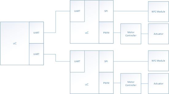
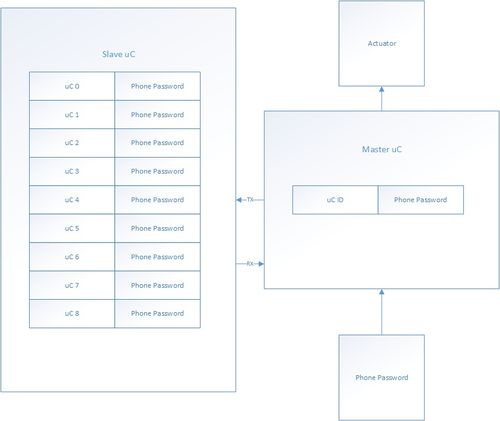
As shown above, the NFC locker system is composed of three uC: Two masters and one shared slave. The two masters drive their independent actuator subsystem, independent NFC module subsystem, and shares the slave.
The masters pull data from its NFC subsystem, and sends the data to the slave. The slave will either accept or reject the password. If the password is verified, the slave will then send information to the master, where the actuator subsystem will either lock or unlock the locker.
Power System Design
| Submodule | Voltage Needed | Voltage Supplier | |
|---|---|---|---|
| 1 | SJOne Board | +5V | ATX Power Supply |
| 2 | NFC Module | +3.3V | SJOne Board |
| 3 | Actuator Submodule | +12V | ATX Power Supply |
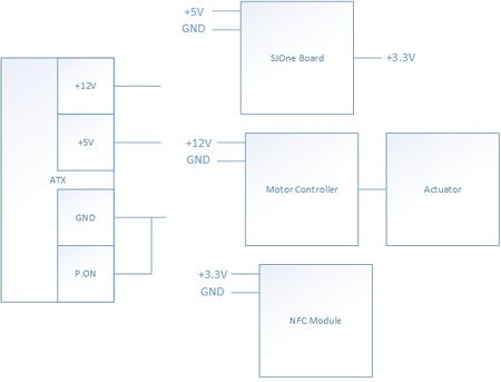
The system ranges in using three different voltages: +12V, +5V, and +3.3V. Because these voltages are standard in computer systems, the team used an ATX power supply. The ATX power supply provides a +12V, +5V, and a +3.3V output.
All ATX power supplies has a "safe power-up" feature in which the power supply will not turn on. In order to turn on the ATX power supply, the P.ON wire must be shorted to ground.
Hardware Interface
In this section, you can describe how your hardware communicates, such as which BUSes used. You can discuss your driver implementation here, such that the Software Design section is isolated to talk about high level workings rather than inner working of your project.
Actuator Subsystem Interface
An actuator can only extend or retract depending on the direction of the signal. With software, The team used a motor controller to change the direction of the PWM signal. Note that one PWM signal must be fully off, while the other must be fully on in order to change the signal's direction.
NFC Interface
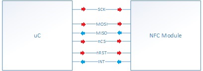
The NFC module can accept High Speed UART (HSU), I2C, or SPI. Out of those three, SPI was chosen for this implementation. In total, seven wires were used to interface the host processor to the PN532. To power the PN532 we used the 3.3v and ground pins available on the SJSU one board. SPI requires three more wires, and the reset and interrupt pins were the last two. The interrupt pin is optional and is not needed for the PN532 to function. The team used the NFC module's interrupt pin because this software's framework is interrupt driven. The interrupt output tells the uC when it is ready. This will be discussed in more detail under the software implementation section for the PN532.
UART Micro-Controller Interface
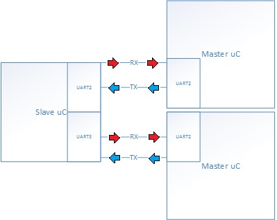
The master uC initiates the communication with the slave. A master uC will send data from the NFC module to the slave uC. The slave will process the data and either send a verification frame or rejection frame to the master which will enable the master to lock or unlock the locker.
Software Design
NFC Software Design
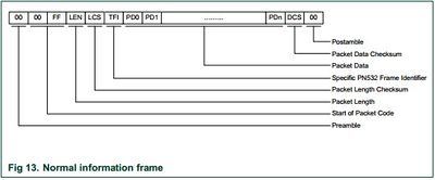
Communication from the host controller between and the PN532 is done with packets. Each Packet is structured as follows:
Where
- Preamble: The start of a packet form Host to PN532
- Start of Packet: The indicator for the start of every packet
- LEN: Length of the packet data including the TFI
- LCS: Checksum for the Length, LEN + LCS = 0x00
- TFI: Frame identifier, 0xD4 for communication from the host to pn532, 0xD5 for communication from the pn532 to the host
- PD#: Byte of the payload
- DCS: Data checksum, TFI + PDO + PD1 + ... + PDN + DCS = 0x00
- Postamble: Ending byte for the frame.
For SPI communication, a byte with the value of 0x01 must also be sent before the packet when transferring packets from the host controller to the PN532.
Packets from the PN532 to the host controller generally do not include the Preamble byte.
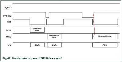
Commands sent form the host controller to the PN532 follow a certain pattern. First the host controller sends a packet to the PN532. Then PN532 then sends an interrupt to the host controller it to receive an acknowledgement (or non acknowledgement) from the PN532. This indicates that the PN532 has registered the send command as valid (or invalid). The PN532 then interrupts the host controller again much later after the command has finished and the host controller can fetch the result for the command. This design uses the interrupt pin, but another system can instead constantly poll the status register of the PN532 to see when it is ready.
Normal Operation of SPI interface:
When the PN532 is turned on (or after the reset pin is inactivated), the PN532 goes into LowVBat mode. When ever the PN532 is in a low power consumption state, it requires some time before the packet can be sent from the host to the PN532. This can be done in two ways with SPI,
- The host controller asserts the chip select pin and wait some time before sending the packet.
- The host controller asserts the H_REQ pin and waits for an interrupt from the PN532 to tell the host it is ready (this was not implemented in this design).
Before the PN532 can start NFC, it needs to be configured into what mode it is going to emulate. This design puts the PN532 into normal mode which will allow for peer-to-peer communication. To do this the packet needs to contain the payload 0x14 (the command), 0x01 (for normal mode), 0xXX (don't care for this byte), and 0x01 (to enable the interrupt). After this is done we can begin to configure the NFC protocols for basic NFC communication.
To configure the NFC as a target, the TgInitAsTarget command needs to be sent from the host processor to the PN532. This design sets the mode of communication to DEP (Data Exchange Protocol) to enable peer-to-peer communication. A ten byte ID is then needed for the PN532 which can be set but should be randomly generated (for this design it is set). Lastly the general bytes need to contain the NFC magic number (0x46666D) and any LLCP (logic link control protocol) the system designer wants to send here. Once this command is sent to the PN532 it will go into power down mode until another NFC device starts the NFC initiation sequence. Once this happens the PN532 will interrupt the host processor (and set its status register to indicate it is ready) and the host processor will receive a NFC status (and possible more) from the host processor. The status will indicate whether or not the packet was accepted by the host processor. The TgSetData and TgGetData can be used to send and receive data to and from the initiator NFC and PN532 module.
In order to send data between and Android phone and the PN532 the host processor needs to process the packets on the LLCP (logic link control protocol). This was not fully implemented (the magic number is required for the phone to respond to the PN532) since there was not enough time to implement this into the system.
If one wishes to implement any NFC device into an embedded system, they should check out http://nfc-forum.org/ and http://www.ecma-international.org/ for more information on the protocols. The PN532 user guide expects its readers to understand much of the protocols of NFC, and these links should provide resources into understanding them.
Phone Application Software Design
The team decided to use the Android platform for our phone application since two of the members had a Samsung Galaxy S4 which made testing on the NFC module much easier. The application's main design principle is simplicity. It's important for the application to be quick and easy to use because a user would want to be able to lock or unlock his/her locker as quickly as possible. The flow of the application begins when you start up the application. The first thing that occurs is that the application will enter the idle state until the user enters a password. After entering a password, the password will then be saved into the application. The phone is actively checking for an NFC device and will keep looping until a device is found. When the user is ready to place the phone near the NFC module, the application will then detect the NFC module and send the password to the module. After sending the password, the phone application then goes back to idle and waits for the next password to be entered. It is up to the module to figure out if the password is correct and what action to take if so.
UART Communication Software Design
Actuator Sub module Software Design
For this actuator's submodule, PWM is needed to control the actuator's state (either extending or retracting). PWM is composed of a frequency and duty cycle. Because the actuator submodule has an "on" or "off" state, the duty cycles used are either 99% (max) or 0% (min). Additionally, frequency is not important for this module
As shown in the hardware implementation of the actuator sub module, in order to extend or retract the actuator, 2 PWM outputs are needed. Each PWM output is connected to the motor controller's inputs. The motor controller inputs dictates the direction of the signal. In order to extend, one PWM1 output must be active, while PWM2 output must be off. Likewise, in order to retract, PWM2 output must be active, while PWM1 output is off.
| Actuator State | Duty Cycle of PWM1 | Duty Cycle of PWM2 | |
|---|---|---|---|
| 1 | Extend | 99% | 0% |
| 2 | Retract | 0% | 99% |
Implementation
NFC Software Implementation
Phone Application Software Implementation
The Android application was relatively easy to implement due to the vast amount of community support for developers. As seen above in the screenshot of the phone application, you can clearly see the simplicity of the application which was one of the design principles. There is a textfield where a user can enter his/her password to open the locker and then hit the save password button. After hitting the save password button, the password is then stored into a string. After the phone detects an NFC device, it uses the Android NFC API to create an NDEF (NFC Data Exchange Format) message that is now ready to be sent. As seen in the screenshot above, when an NFC device is detected, the phone application will display on the screen "Touch to beam". After touching the application, it will now send the password to the NFC module on the locker. The microcontroller on the locker will now decide the next action.
UART Communication Software Implementation
This system consists a master and a slave. Though using one of the master's UART ports, the master sends its locker ID(1 byte) and the phone's password(4 bytes) as a password. The slave will receive the 5 bytes of data and search its pre-defined array for the that unique password. The slave will then send 1 byte to the master distinguishing if the password is valid or not.
Actuator Software Implementation
Testing & Technical Challenges
Describe the challenges of your project. What advise would you give yourself or someone else if your project can be started from scratch again? Make a smooth transition to testing section and described what it took to test your project.
Include sub-sections that list out a problem and solution, such as:
Testing
Android Application
The first set of testing was dedicated to the Android application because it was one of the first task completed and that could be tested on its own. In order to test our application, we just used another Android phone to receive the NDEF message being sent. We were able to successfully validate our phone application when we were able to send and receive our "locker password" between two NFC-capable phones.
NFC Module
Testing the NFC Module required an NFC enabled phone. It would act as the initiator and would be brought to the NFC module after the PN532 was set as a target. The resultant packets sent from the PN532 to the host processor were then output to a computer via USB. The output was then presented to us for analysis with the application Hercules.
Locking System
To test our locking system, we hooked up our microcontrollers, motor driver controller boards, and actuators. The actuators were then toggled to show the functionality of the locking system.
Technical Challenges
NFC Module
The most difficult part of this project was to get the NFC module to work as intended. Connecting everything was straightforward since everything was labeled on the NFC module. However, figuring out how to actually integrate the NFC module into our locker system was extremely difficult because it requires a deep and existing knowledge of NFC. In addition to just NFC knowledge, there was a lot of overhead because we had to also know about networking. Trying to get the NFC module to work took extensive hours of reading the datasheet and researching online about what was being read.
Ethernet
Initially, our goal for the networking portion of our locker system was to use Ethernet. This is because Ethernet provides high speed, long range, and the ability to expand if we were to add additional lockers. However, after working on integrating the Ethernet module into our system, we discovered that there was too much overhead for the scope of our project. We decided that it would be best to just use UART for this project, but Ethernet would definitely be something we would use if we wanted to improve our project.
Android Application
At first, developing the Android application was slightly difficult because none of the team members had any experience in developing a phone application. However, after reading the Android Developers page and using Google to find the answer to other questions, the phone application started developing nicely. The Android Developers page had an excellent guide to NFC basics. Using Google search, we were able to find out how to properly integrate a textfield and button into our application.
Conclusion
Coming into this project we didn't expect NFC to be nearly as complicated as it was, and the lack of knowledge about it hindered the development in this project. The PN532 does a good job of doing much of the work for NFC specific protocol and physical layers. Unfortunately in order to interface with the Android phone we would need to fully implement the NFC LLCP standard, which we learned about too late. We were unable to access the full data sheet for the PN532 but we were able to access the user guide. Unfortunately the actual protocols were referred to by their acronyms, and finding the documentation to give the description of these protocols took time. After taking the time to understand these protocols we were able to generate responses from the phone but were unable to understand the data that was sent to us. It took more time to discover that LLCP was required to communicate to an Android device. By the time we finished researching LLCP, we were out of time for the project.
Ultimately, our project idea might have been a bit too ambitious for our scope of knowledge. Working with the NFC module required an extensive knowledge of NFC and networking. In addition, there is not much documentation or community help with regards to NFC as compared to making the Android application.
Project Video
Upload a video of your project and post the link here.
Project Source Code
Send me your zipped source code and I will upload this to SourceForge and link it for you.
References
Acknowledgement
We would like to acknowledge Preetpal Kang and Dr. Haluk Özemek.
