Lab Assignments
GPIO
Objective
Interface your LPC17xx to a switch and an LED.
Although the interface may seem simple, you do need to consider hardware design and know some of the fundamental of electricity. There are a couple of goals for us :
- No hardware damage if faulty software is written.
- Circuit should prevent excess amount of current to avoid processor damage.
Required Background
- You should know how to bit-mask variables
- You should know how to wire-wrap
- You should know fundamentals of electricity and the famous V = IR equation.
GPIO
|
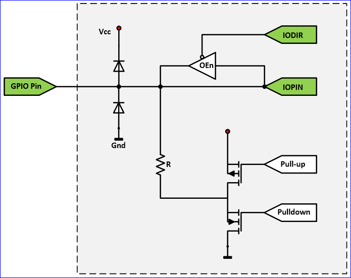
GPIO stands for "General Purpose Input Output". Each pin can at least be used as an output or input. In an output configuration, the pin voltage is either 0v or 3.3v. In input mode, we can read whether the voltage is 0v or 3.3v. You can locate a GPIO that you wish to use for a switch or an LED by first starting with the schematic of the board. The schematic will show which pins are "available" because some of the microcontroller pins may be used internally by your development board. After you locate a free pin, such as P2.0, then you can look-up the microcontroller user manual to locate the memory that you can manipulate. |
Coding
Hardware Registers
The hardware registers map to physical pins. If we want to attach our switch and the LED to our microcontroller's PORT0, then here are the relevant registers and their functionality :
| LPC_GPIO0->FIODIR | Direction of the port pins, 1 = output |
| LPC_GPIO0->FIOPIN |
Read : Sensed inputs of the port pins, 1 = HIGH Write : Control voltage level of the pin, 1 = 3.3v |
| LPC_GPIO0->FIOSET | Write only : Any bits written 1 are OR'd with FIOPIN |
| LPC_GPIO0->FIOCLR | Write only : Any bits written 1 are AND'd with FIOPIN |
Switch
/* Make direction of PORT0.2 as input */
LPC_GPIO0->FIODIR &= ~(1 << 2);

/* Now, simply read the 32-bit FIOPIN registers, which corresponds to
 * 32 physical pins of PORT0.  We use AND logic to test if JUST the
 * pin number 2 is set
 */
if (LPC_GPIO0->FIOPIN & (1 << 2)) {
    // Switch is logical HIGH
}
else {
    // Switch is logical LOW
} |
Note that the "inline" resistor is used such that if your GPIO is mis-configured as an OUTPUT pin, hardware damage will not occur from badly written software. |
LED
/* Make direction of PORT0.3 as OUTPUT */
LPC_GPIO0->FIODIR |= (1 << 3);

/* Setting bit 3 to 1 of IOPIN will turn ON LED
 * and resetting to 0 will turn OFF LED.
 */
LPC_GPIO0->FIOPIN |= (1 << 3);

/* Faster, better way to set bit 3 (no OR logic needed) */
LPC_GPIO0->FIOSET = (1 << 3);

/* Likewise, reset to 0 */
LPC_GPIO0->FIOCLR = (1 << 3); |
Given below are two configurations of an LED. Usually, the "sink" current is higher than "source", hence the active-low configuration is used more often. |
Assignment
At the end of this lab, you should be familiar with how a microcontroller's memory can access physical pins. Test your knowledge by doing the following:
- Interface your board's pin to an external switch
- Interface your board's pin to an LED
- If the switch is pressed, light up an LED
- Do not use any pre-existing library such as a GPIO class
UART
Introduction
The objective of this lesson is to understand UART, and use two boards and setup UART communication between them.
UART stands for Universal Asynchronous Receiver Transmitter. There is one wire for transmitting data, and one wire to receive data. A common parameter is the baud rate known as "bps" which stands for bits per second. If a transmitter is configured with 9600bps, then the receiver must be listening on the other end at the same speed.
UART is a serial communication, so bits must travel on a single wire. If you wish to send a char over UART, the char is enclosed within a start and a stop bit, so to send 8-bits of char data, it would require 2-bit overhead; this 10-bit of information is called a UART frame. Let's take a look at how the character 'A' is sent over UART. In ASCII table, the character 'A' has the value of 65, which in binary is: 0100-0001. If you inform your UART hardware that you wish to send this data at 9600bps, here is how the frame would appear on an oscilloscope :
A micrcontroller can have multiple UARTs in its hardware, and usually UART0 is interfaced to a "USB to serial" converter chip which is then connected to your computer. In this exercise, you will write a driver for UART-2 and attempt to communicate between two boards.
I encourage you to fully read this article first, and here is a video about the UART0 tutorial. This is a FAST PACED video, so learn to pause the video and look over your LPC user manual frequently :) Note that I forgot to configure the PINSEL registers, which are covered by this tutorial below.
UART Pins
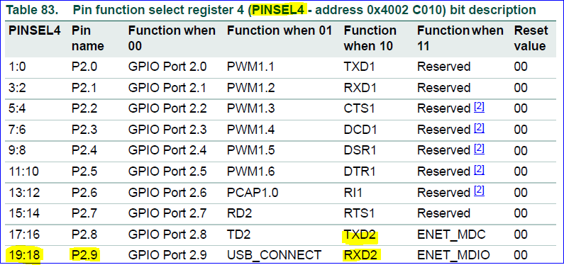
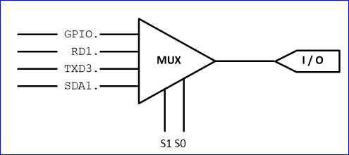
Before you write a UART software driver, you need to understand the physical constraints and identify the UART pins on your processor. A GPIO (general purpose input output) is a multi-purpose pin, and certain pins are used for certain functions. For example, P0.0 and P0.1 on your LPC17xx processor can be used for an LED (output), a switch (input), or as UART transmitter and receive signals. We will configure the microcontroller's internal MUX (multiplexor) to connect internal UART to external pins.
Clock System & Timing
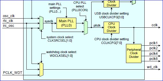
A crystal drives a processor clock, and it is usually less than 20Mhz. A processor usually uses a "PLL" or "phased-lock-loop" to generate a faster clock than the crystal. So, you could have a 4Mhz clock, and the PLL can be used to internally multiply the clock to provide 48Mhz to the processor. The same 48Mhz is then fed to processor peripherals, and sometimes you have a register that can divide this higher clock to slower peripherals that may not require a high clock rate. Remember that lower clock speed means lower power consumption.
9600bps means that one bit takes 1/9600 = 104uS (micro-seconds) per bit. The idea is that we want to divide the peripheral clock to UART hardware by a number that yields roughly 104uS per bit. The Software Driver section goes over how to configure your UART driver to divide the clock to yield the desired baud rate.
Hardware Design
There is not much hardware design other than to locate UART-2 pins on your processor board and connecting these wires to the second board. Each pin on a microcontroller may be designed to provide specific feature. So the first thing to do is identify which physical pins can provide UART-2 signals.
After you identify the physical pins, you would connect these pins to the second board. Remember that your TX pin should be connected to second board's RX pin and vice versa. Connecting two TX pins together will damage your processor. After you connect the Rx/Tx pairs together, you also need to connect the ground wire of two boards together. Not connecting the ground reference together is essentially like asking the other board "How far is my hand from the ground" when the ground reference is missing.
Software Driver
|
The UART chapter on LPC17xx has a really good summary page on how to write a UART driver. Read the register description of each UART register to understand how to write a driver. This tutorial gives away answers but unless you spend 1-2 hours reading the UART chapter, you will forget this knowledge. The datasheet shows many registers but remember that for a simple driver, we will not need interrupts so you can skip the sections that talk about the UART interrupts.
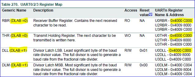
Notice that four registers have the same address. The UART divider registers are only accessible if DLAB bit is 1; this was done to protect accidental change of baud rate. Furthermore, notice that the CPU is intelligent enough to know if you are accessing the RX or the TX register based on if the register is being read or written. void uart0_init(void)
{
LPC_SC->PCONP |= (1 << 3); // Enable power to UART0
LPC_SC->PCLKSEL0 &= ~(3 << 6);
LPC_SC->PCLKSEL0 |= (1 << 6); // Uart clock = CPU / 1
LPC_PINCON->PINSEL0 &= ~(0xF << 4); // Clear values
LPC_PINCON->PINSEL0 |= (0x5 << 4); // Set values for UART0 Rx/Tx
LPC_UART0->LCR = (1 << 7); // Enable DLAB
/* See the formula picture to get more info.
* Default values of fractional dividers simplifies the equation
* Warning: You need to set DLM/DLL correctly, but if divider is small enough, it will fit inside DLL
*/
LPC_UART0->DLM = 0;
LPC_UART0->DLL = CPU_CLOCK / (16 * 9600) + 0.5);
LPC_UART0->LCR = 3; // 8-bit data
} |
char uart0_putchar(char out)
{
    LPC_UART0->THR = out;
    while(! (LPC_UART0->LSR & (1 << 6)));
    return 1;
}
To send a char over UART, the code looks incredibly easy; just two lines! It is supposed to be very easy because the UART hardware is supposed to handle the UART frame, and send start bit, followed by 8-data bits, and a stop bit by simply writing the THR register. The moment you write this register, the hardware will start shifting bits out of the wire. The while loop is present because after you write the THR register, we want to wait until hardware is done sending the bits out of the wire otherwise writing the same register again will corrupt the on-going transfer.
Advanced Design
What you've done so far is wrote a polling UART driver. If you used 9600bps, and sent 1000 characters, your processor would basically enter a "busy-wait" loop and spend 1040ms to send 1000 bytes of data. You can enhance this behavior by allowing your uart_putchar() function to enter data to a queue, and return immediately, and you can use the "THRE" or "Transmitter Holding Register Empty" interrupt indicator to remove your busy-wait loop while you wait for a character to be sent.
Assignment
- Locate the physical pins for a UART that is not already used by your board
- Configure the PINSEL to use the pins for UART Rx/Tx
- Initialize your UART at any baud rate
- Write uart_putchar(char) and uart_getchar() functions
- Interface your UART with someone else's board, and test the communication.
SPI
SPI BUS
SPI stands for Serial Peripheral Bus. It is a high-speed, full-duplex bus that uses minimum of 3 wires to exchange data. The popularity of this bus rose when SD cards (and its variants ie: micro-sd) officially supported this bus according to the SD specifications. Furthermore, unlike UART in which you can only have one transmitter and a receiver, SPI bus can have one master and multiple slave devices.
SPI Bus Signals
|
The CS signal selects one slave, and the slave takes over the MISO pin. If a slave is not selected, then it shall leave the MISO pin in hi-z state. If multiple slaves have their CS signal asserted, they will try to take control of the MISO pin and damage their MISO pins. For example, if one slave drives the signal high (connect to 3.3v) and the other drives it low (connect to ground), then short-circuit will occur damaging this pin.
The SCK signal can reach speed of 24Mhz and beyond, however, SD cards are usually limited to 24Mhz according to the specifications. Furthermore, any signal over 24Mhz on a PCB requires special design consideration to make sure it will not deteriorate, thus 24Mhz is the usual maximum. Furthermore, you need a CPU twice as fast as the speed you wish to run to support it. For example, to run at 24Mhz SPI, we need 48Mhz CPU or higher. Because each wire is driven directly (rather than open-collector), higher speeds can be attained compared to 400Khz I2C bus.
Hardware
Suppose that you wanted to interface a single SPI bus to three SD cards, the following will need to be done :
- Connect all MOSI, MISO, and SCK lines together
- Connect individual CS lines of three SD cards to SPI master (your processor)
It is also recommended to provide a weak pull-up resistor on each of the SPI wires otherwise some devices like an SD card may not work. 50K resistor should work, however, lower resistor value can acheive higher SPI speeds.
Software Driver
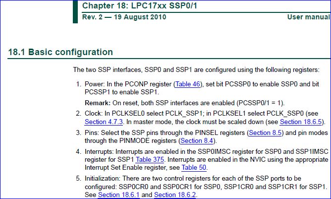
Unlike UART, the SPI driver is incredibly easy. The SPI is labeled as SSP on LPC17xx datasheet due to historic reasons, and this chapter in the datasheet shows the software setup very well. After the SPI is initialized on the hardware pins, the next steps is to write an spi function that will exchange a byte. Note that if the master wants to receive data, it must send a data byte out to get a data byte back. The moment we write to the DR (data register) of the SPI peripheral, the MOSI will begin to send out the data. At the same time, the MISO will capture the data byte back to the same DR register. In other words, SPI bus is a forced full-duplex bus.
void spi1_Init()
{
    LPC_SC->PCONP |= (1 << 10);     // SPI1 Power Enable
    LPC_SC->PCLKSEL0 &= ~(3 << 20); // Clear clock Bits
    LPC_SC->PCLKSEL0 |=  (1 << 20); // CLK / 1

    // Select MISO, MOSI, and SCK pin-select functionality
    LPC_PINCON->PINSEL0 &= ~( (3 << 14) | (3 << 16) | (3 << 18) );
    LPC_PINCON->PINSEL0 |=  ( (2 << 14) | (2 << 16) | (2 << 18) );

    LPC_SSP1->CR0 = 7;          // 8-bit mode
    LPC_SSP1->CR1 = (1 << 1);   // Enable SSP as Master
    LPC_SSP1->CPSR = 8;         // SCK speed = CPU / 8
}

char spi1_ExchangeByte(char out)
{
    LPC_SSP1->DR = out;
    while(LPC_SSP1->SR & (1 << 4)); // Wait until SSP is busy
    return LPC_SSP1->DR;
} |
Multitasking Warnings
If your software runs multiple tasks, and these tasks can access SPI, care needs to be taken because if two CS signals are asserted at the same time, hardware damage will occur. This leads to the topic of using a mutex (semaphore) under FreeRTOS and you can read the FreeRTOS tutorial to learn more.
SJ-One Board Driver Instructions
Preparation for the SPI driver:
- Note that when we refer to "SPI", it also means "SSP" in the LPC user manual
- Study the schematic, and take a note of which pins have the SSP1 or SPI#1 peripheral pin-out. Note this down or draw this out.
- Study and read the SSP1 LPC user manual chapter a few times
- Study the schematic, and locate the CS pin for the SPI flash attached to SSP1, then write a simple GPIO driver for this to select and deslect this pin
- Read the SPI flash datasheet that shows the SPI transactions for read/write, signature read etc.
- Rev4 board has Adesto flash, and previous revisions have Atmel flash.
Writing the driver:
- First, initialize the pin MUX using the PINSEL register. I believe the PINSEL register is part of the LPC_PINCON struct
- Read the SSP1 chapter, and follow the steps on the first page to power on the SSP peripheral, and then initialize the CR0 and the CR1 register to perform SPI master initializationaa
- Now, write the spi exchange byte function using the DR and the SR (status) register.
Assignment
- Write a driver for SSP#1
- This SPI is interfaced to SD card and SPI Flash memory
- You need just an
init()routine along withchar byte_transfer(char)function.
- Identify the pin for SPI flash memory's chip-select signal (CS)
- Read the SPI flash memory datasheet and read the signature of this device and display it using printf()
- This should be at
SJSU_Dev\ref_and_datasheets\datasheets
- This should be at
- Read the SPI Flash memory's status register and print information about each bit in a nicely formatted output.
- This isn't the SPI peripheral status register, read the SPI flash memory datasheet.
- Extra credit:
- Read page zero (first 512 bytes), and print the following:
- Number of bytes per sector, number of sectors per cluster, and the total number of sectors.
- Hint: Use this: FAT info
- Hint#2: You can use the API from spi_flash.h
- Read page zero (first 512 bytes), and print the following:
FAT Information
Information about the FAT boot sector and MBR
The first sector of the flash contains a Master Boot Record (MBR) which has pointers to where the partitions are placed in the storage device. Please have a look at this link for the structure of MBR. The first 446 bytes is the bootstrap code area. After that there is a partition table with four entries and then a boot signature (0x55AA). Each entry is 16 bytes long and you can find the layout of each entry here.
One of the fields in the partition entry is "partition type". This should tell us what type of filesystem is resident on the partition. In our case it should be FAT12 (0x01). The last 8 bytes in the partition entry will tell us the Logical Block Address (LBA) of the first absolute sector in the partition and the total number of sectors in the partition. Essentially, we want to read the sector pointed to by this LBA for the FAT boot sector. That sector will give us the required information (no of clusters, total sectors, etc.. ).
I2C
Theory of Operation
I2C is prounced "eye-squared see". It is also known as "TWI" because of the intial patent issues of this BUS. This is a popular, low throughput (100-1000Khz), half-duplix BUS that only uses two wires regardless of how many devices are on this BUS. Many sensors use this BUS because of its ease of adding to a system.
Open-Collector BUS
I2C is an open-collector BUS, which means that no device shall have the capability of internally connecting either SDA or SCL wires to power source. The communication wires are instead connected to the power source through a "pull-up" resistor. When a device wants to communicate, it simply lets go of the wire for it to go back to logical "high" or "1" or it can connect it to ground to indicate logical "0".
Pull-up resistor
Using a smaller pull-up can acheiver higher speeds, but then each device must have the capability of sinking that much more current. For example, with a 5v BUS, and 1K pull-up, each device must be able to sink 5mA.
Protocol Information
I2C was designed to be able to read and write memory on a slave device. The protocol may be complicated, but a typical "transaction" involving read or write of a register on a slave device is simple granted a "sunny-day scenario" in which no errors occur.
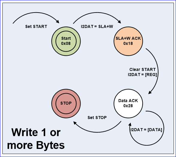
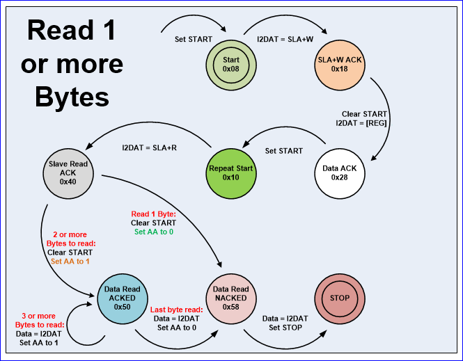
The code given below illustrates I2C transaction split into functions, but this is the wrong way of writing an I2C driver. An I2C driver should be "transaction-based" and the entire transfer should be carried out using a state machine. The idea is to design your software to walk the I2C hardware through its state to complete an I2C transfer.
In the diagrams given below, your software should take the step given in the arrow, and the hardware will go to the next state granted that no errors occur. To implement this in your software, you should follow the following steps :
- Perform the action given by the arrow
- Clear the "SI" (state change) bit for HW to take the next step
- Wait for "SI" (state change) bit to set, then take the next action
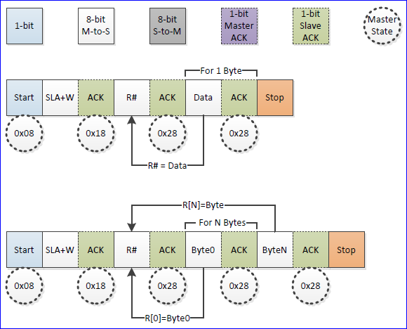
The master will always initiate the transfer, and the device reading the data should always "ACK" the byte. For example, the master sends the 8-bit address after the START condition and the addressed slave should ACK the 9th bit (pull the line LOW). Likewise, when the master sends the first byte after the address, the slave should ACK that byte if it wishes to continue the transfer.
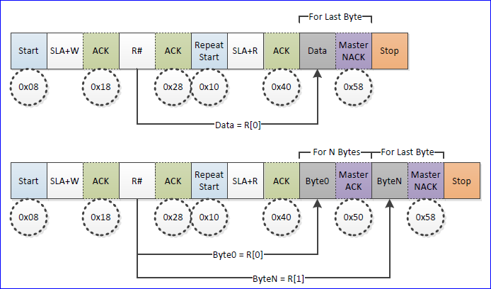
When the master enters the "read mode" after transmitting the read address after a repeat-start, the master begins to "ACK" each byte that the slave sends. When the master "NACKs", it is an indication to the slave that it doesn't want to read anymore bytes from the slave.
Write Transaction
| Code Sample | State Machine |
|
A typical I2C write is to be able to write a register or memory address on a slave device. Here are the steps:
To maximize throughput and avoid having to do this for each memory location, the memory address is considered "starting address". If we continue to write data, we will end up writing data to M, M+1, M+2 etc. The ideal way of writing an I2C driver is one that is able to carry out an entire transaction given by the function below. Note that the function only shows the different actions hardware should take to carry out the transaction, but your software should be state machine based as illustrated on the state machine diagram on the right.
void i2c_write_slave_reg(void)
{
    i2c_start();
    i2c_write(slave_addr);
    i2c_write(slave_reg);
    i2c_write(data);

    /* Optionaly write more data to slave_reg+1, slave_reg+2 etc. */
    // i2c_write(data); /* M + 1 */
    // i2c_write(data); /* M + 2 */

    i2c_stop();
} |
Read Transaction
| Code Sample | State Machine |
|
An I2C read is slightly more complex and involves more protocol to follow. What we have to do is switch from "write-mode" to "read-mode" by sending a repeat start, but this time with an ODD address. To simplify things, you can consider an I2C even address being "write-mode" and I2C odd address being "read-mode". Again, the function shows what we want to accomplish. The actual driver should use state machine logic to carry-out the entire transaction.
void i2c_write_slave_reg(void)
{
    i2c_start();
    i2c_write(slave_addr);
    i2c_write(slave_reg);

    i2c_start();                  // Repeat start
    i2c_write(slave_addr | 0x01); // Odd address

    char data = i2c_read(0);      // NACK if reading last byte

    /* If we wanted to read 3 register, it would look like this:
     * char d1 = i2c_read(1);
     * char d2 = i2c_read(1);
     * char d3 = i2c_read(0);
     */

    i2c_stop();
} |
I2C Slave State Machine Planning
Before you jump right into the assignment, do the following:
- Read and understand how an I2C master performs slave register read and write operation
- Look at existing code to see how the master operation handles the I2C state machine function
- This is important so you can understand the existing code base
- Next to each of the master state, determine which slave state is entered when the master enters its state
- Determine how your slave memory or registers will be read or written
It is important to understand the states, and use the datasheet to figure out what to do in the state to reach the next desired state given in the diagrams below.
Master Write
In the diagram below, note that when the master sends the "R#", which is the register to write, the slave state machine should save this data byte as it's INDEX location. Upon the next data byte, the indexed data byte should be written.
Master Read
In the diagram below, the master will write the index location (the first data byte), and then perform a repeat start. After that, you should start returning your indexed data bytes.
Assignment
Extend the I2C base class to also support slave operation. Test your I2C driver by using one board as a master, and another board as a slave.
- Study
i2c_base.cpp, particularly the following methods:-
init() -
i2cStateMachine()- Note that this function is called by the hardware interrupt asynchronously whenever I2C state changes.
- The other I2C master will simply "kick off" the START state, and this function carries the hardware through its states to carry out the transaction.
- The functions you add to this base class are accessible by the I2C2 instance.
-
- Add
initSlave()method to the I2C to initialize the slave operation.- Allow the user to supply a memory to be read or written by another master.
- Extend the state machine for I2C slave operation.
- Study the CPU user manual first, and create a state machine diagram on paper.
- The first register supplied after the slave address should be used as an "offset" of the memory to read or write.
- Demonstrate the following :
- Demonstrate that you are able to read and write the slave memory.
- For extra credit and bragging rights, create state machine diagrams, and if you can make better ones, I will use your diagrams at this wikipedia page :)
Sample Code
#include "i2c2.hpp"
#include <stdint.h>
#include <stdio.h>

int main(void)
{
    I2C2& i2c = I2C2::getInstance(); // Get I2C driver instance
    const uint8_t slaveAddr = 0xC0;  // Pick any address other than the used used at i2c2.hpp
    uint8_t buffer[256] = { 0 };     // Our slave read/write buffer

    // high_level_init() will init() I2C, let's init slave
    i2c.initSlave(slaveAddr, &buffer, sizeof(buffer));

    // I2C interrupt will (should) modify our buffer.
    // So just monitor our buffer, and print and/or light up LEDs
    // ie: If buffer[0] == 0, then LED ON, else LED OFF
    uint8_t prev = buffer[0];
    while(1)
    {
        if (prev != buffer[0]) {
            prev = buffer[0];
            printf("buffer[0] changed to %#x\n", buffer[0]);
        }
    }

    return 0;
}
Warning
Since the I2C state machine function is called from inside an interrupt, you may not be able to to use printf(), especially if you are running FreeRTOS. As an alternative, use the debug printf methods from the printf_lib.h file.
Interrupts
Introduction
This tutorial demonstrates how to use interrupts on a processor. In general, you will understand the concept behind interrupts on any processor, but we will use the SJ-One board as an example.
What is an interrupt?
- Hardware capability to break normal software flow to attend an urgent request
- "An event that needs immediate attention"
Science
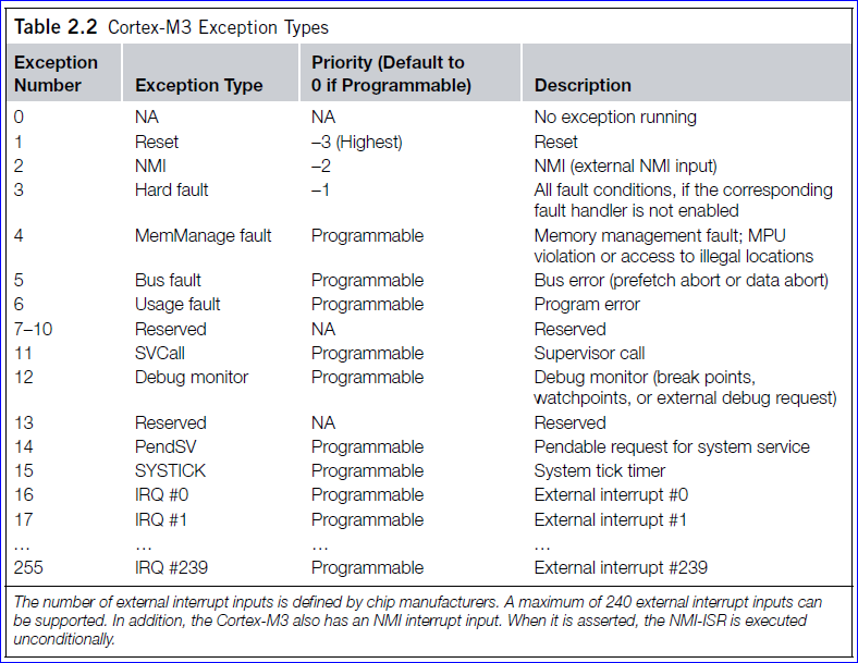
The science behind interrupts lies in the hardware that allows the CPU to be interrupted. Each peripheral in a microcontroller may be able to assert an interrupt to the CPU core, and then the CPU core would jump to the corresponding interrupt service routine (ISR) to service the interrupt.
ISR Procedure
The following steps demonstrate what happens when an interrupt occurs :
- CPU manipulates the PC (program counter) to jump to the ISR
- IMPORTANT: CPU will disable interrupts (or that priority level's interrupts until end of ISR)
- Registers are saved before running the ISR (pushed onto the stack)
- ISR is run
- Registers are restored (popped from stack)
- Interrupts are re-enabled (or that priority level's interrupt is re-enabled)
On some processors, the savings and restoring of registers is a manual step and the compiler would help you do it. You can google "GCC interrupt attribute" to study this topic further. On SJ-One board, which uses LPC17xx (ARM Cortex M3), this step is automatically taken care of by the CPU hardware.
The SW to HW Connection
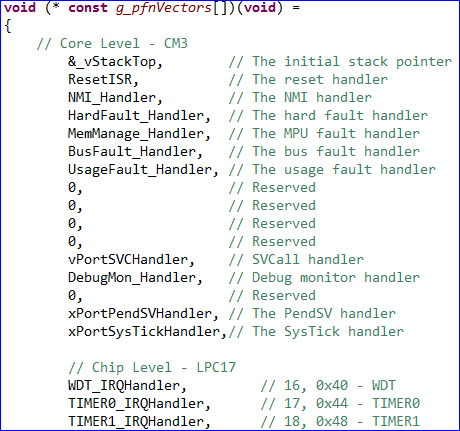
Now that we understand how the CPU hardware services interrupts, we need to define how we inform the CPU WHERE our ISR function is located at. There is something called an Interrupt Vector Table. This table is nothing but addresses of functions that correspond to the microcontroller interrupts. Specific interrupts use specific "slots" in this table, and we have to populate these spots with our software functions that service the interrupts.
SJ-One (LPC17xx) Example
Through some magic of the compiler, and the linker script, the compiler is able to place the software interrupt vector table at a specific location that the CPU expects the interrupt vector table to be located at. This connects the dots about how the CPU is able to determine WHERE your interrupt service routines are located at. From there on, anytime a specific interrupt occurs, the CPU is able to fetch the address and make the JUMP.
GCC Magic
In the SJ-One sample project, each ISR is named, but is labeled as a "weak" function. What this means in the land of GCC (compiler) is that unless the same function name is defined somewhere else, the weak function serves as the ISR function. If you do define the function name somewhere else, it will override the "weak" function and the compiler will place the address of your new function into the interrupt vector table.
Setup ISR on SJ-One
The first step is to be able to locate the real-name of the "weak" ISR function. For example, you can locate a UART0 ISR function that is weak, and we will override with our new function. The only thing to keep in mind is that due to "C++ Mangling" of function names, if your ISR is located in a *.cpp file, you will need to enclose it into extern "C" tags. See below for examples:
/***************/
/* my_file.cpp */

    extern "C"
    {
        void UART0_IRQHandler()
        {
            /* Your ISR */
        }
    }

/*************/
/* my_file.c */

    /* extern tag not needed for a C file */
    void UART0_IRQHandler()
    {
        /* Your ISR */
    }
What to do inside an ISR
Do very little inside an ISR. When you are inside an ISR, the whole system is blocked (other than higher priority interrupts). If you spend too much time inside the ISR, then you are destroying the realtime operating system principle and everything gets clogged because of you :(
With that said, here is the general guideline
- Spend as little time as possible. DO NOT POLL FOR ANYTHING.
- If you are using FreeRTOS API, you must use FromISR functions only!
- Most important: Clear the source of the interrupt
- For example, if interrupt was for rising edge of a pin, clear the "rising edge" bit such that you will not re-enter into the same interrupt function.
ISR processing inside a FreeRTOS Task
It is a popular scheme to have an ISR quickly exit, and then resume a task or thread to process the event. For example, if we wanted to write a file upon a button press, we don't want to do that inside an ISR because it would take too long and block the system. What we can do instead is have the ISR "give" a semaphore, and a task to block upon a semaphore.
What you may argue with the example below is that we do not process the ISR immediately, and therefore delay the processing. But you can tackle this scenario by resuming a HIGHEST priority task. Immediately, after the ISR exits, due to the ISR "yield", FreeRTOS will resume the high priority task immediately rather than servicing another task.
/* Declare and create the semaphore in main() */
SemaphoreHandle_t gButtonPressSemaphore = NULL;

void my_button_press_isr(void)
{
    long yield = 0;
    xSemaphoreGiveFromISR(gButtonPressSemaphore, &yield);
    portYIELD_FROM_ISR(yield);
}

void button_press_task(void *p)
{
    while(1) {
        if (xSemaphoreTake(gButtonPressSemaphore, portMAX_DELAY)) {
            /* Process the interrupt */
        }
    }
}

void main(void)
{
    gButtonPressSemaphore = xSemaphoreCreateBinary();

    /* TODO: Hook up my_button_press_isr() using eint.h */

    /* TODO: Create button_press_task() and start FreeRTOS scheduler */
}
Assignment
Write the implementation of eint.c from scratch. Before you get any ideas, and to make sure you are not biased, just erase this file and begin with an empty mind.
- From the
startup.cppfile, identify the name of the function for EINT3- This interrupt function is used for Port0 and Port2 interrupts
- When either EINT3, Port0, or Port2 interrupt occurs, this function will execute
- Allow the user to specify the pin number and a callback function.
- When the interrupt occurs, make the callback for the user function
- Test your implementation
- Attach a couple of switches on Port2, and ensure that the callbacks are made correctly.
- If SW1 is pressed, it should go to callback1
- If SW2 is pressed, it should go to callback2
- Hints:
- LPC_GPIOINT structure can configure rising or falling edges for Port0 and Port2
- You must CLEAR the source of interrupt by using either IO0IntClr or IO2IntClr otherwise your interrupt will go to an infinite loop.
- You cannot use
printf()to print anything from inside an ISR (if FreeRTOS is running), but you can use the API fromprintf_lib.h
FreeRTOS Tasks
The objective of this assignment is to show you how to create a FreeRTOS task a few different ways. The FreeRTOS Tutorial is definitely a must read before going through this lesson.
FreeRTOS "Hello World" Task
A task just needs memory for its stack and an infinite loop. To prevent "hogging" the CPU, you should use a delay such that the CPU can be allocated to other tasks. Here is the simplest FreeRTOS task:
void hello_world_task(void* p)
{
    while(1) {
        puts("Hello World!");
        vTaskDelay(1000);
    }
}

int main()
{
    xTaskCreate(hello_world_task, (signed char*)"task_name", STACK_BYTES(2048), 0, 1, 0);
    vTaskStartScheduler();

    return -1;
}
C++ based FreeRTOS task
As a project gets more complex, it becomes difficult to manage initialization and share queue or semaphore handles. This was the motivation to create a C++ based FreeRTOS task.
A task can "share" its pointers, handles, or "objects" with another task by name. This way, we don't have to worry about declaring handles into a common header file, hence we do not plague the global namespace :) See the next examples on how a task can share a handle with another task by an intuitive string name.
C++ Task
/// IDs used for getSharedObject() and addSharedObject()
typedef enum {
   shared_SensorQueueId,
} sharedHandleId_t;

/// Orientation type enumeration
typedef enum {
    invalid,
    left,
    right,
} orientation_t;

class orient_compute : public scheduler_task
{
    public:
        orient_compute(uint8_t priority) : scheduler_task("compute", 2048, priority)
        {
            /* We save the queue handle by using addSharedObject() */
            QueueHandle_t my_queue = xQueueCreate(1, sizeof(orientation_t));
            addSharedObject(shared_SensorQueueId, my_queue);
        }

        bool run(void *p)
        {
            /* Compute orientation here, and send it to the queue once a second */
            orientation_t orientation = invalid;
            xQueueSend(getSharedObject(shared_SensorQueueId), &orientation, portMAX_DELAY);

            vTaskDelay(1000);
            return true;
        }
};

class orient_process : public scheduler_task
{
    public:
        orient_process (uint8_t priority) : scheduler_task("process", 2048, priority)
        {
            /* Nothing to init */
        }

        bool run(void *p)
        {
            /* We first get the queue handle the other task added using addSharedObject() */
            orientation_t orientation = invalid;
            QueueHandle_t qid = getSharedObject(shared_SensorQueueId);

            /* Sleep the task forever until an item is available in the queue */
            if (xQueueReceive(qid, &orientation, portMAX_DELAY))
            {
            }

            return true;
        }
};
Note that a better design is to minimize the use of getSharedObject(). So it is recommended that the creator of the handle add the shared object in its init(), and other tasks can store the handle in their taskEntry() function.
Add the task in main()
int main()
{
    scheduler_add_task(new orient_compute(PRIORITY_LOW));
    scheduler_add_task(new orient_process(PRIORITY_LOW));
    scheduler_start();
    return 0;
}
Assignment
This assignment is based on SJ-One board, but you can alter the requirement to fit your own hardware.
- Create a task (task1) that computes the orientation of the board.
- You can use the acceleration sensor to figure out the orientation of the board
- Send the orientation enumeration, such as "up", "down", "left", "right" to a queue every 1 second
- Create another task (task2) that waits on the queued item
- If the orientation is left or right, light up the LEDs (otherwise turn them off)
- Note down the observations by doing the following:
- Print a message before and after sending the orientation to the queue
- Print a message after the second task receives an item from the queue
- Use the same priority for both tasks, and note down the order of the print-outs
- Use higher priority for the receiving task, and note down the order of the print-outs.
- Create a terminal command: "orientation on" and "orientation off"
- If orientation is commanded on, resume the task1, otherwise suspend it
- See code below on hints of how this command can get control of another task.
- Answer the following questions:
- What if you use ZERO block time while sending an item to the queue, will that make any difference?
- What is the purpose of the block time during xQueueReceive() ?
// At the terminal tasks taskEntry() function :
bool terminalTask::taskEntry()
{
    cp.addHandler(orientationCmd,  "orientation", "Two options: 'orientation on' or 'orientation off'");
}

// Somewhere else:
CMD_HANDLER_FUNC(orientationCmd)
{
    // Our parameter was the orientation tasks' pointer, but you may want to check for NULL pointer first.
    scheduler_task *compute = scheduler_task::getTaskPtrByName("compute");

    // You can use FreeRTOS API or the wrapper resume() or suspend() methods
    if (cmdParams == "on") {
        vTaskResume(compute->getTaskHandle());  // Can also use: compute->resume();
    }
    else {
        vTaskSuspend(compute->getTaskHandle()); // Can also use: compute->suspend();
    }

    return true;
}
FreeRTOS Application Programming
In this project, we will attempt to "combine" all the FreeRTOS knowledge into a single assignment.
After completing the assignment, you will get a sense of how the CPU is utilized, and how to use a new FreeRTOS event group API. All together, you should achieve a better sense of designing your tasks and using the File I/O for debugging purposes.
Assignment
Please follow the steps precisely in order to complete the objectives of the assignment. If you use the C++ FreeRTOS framework, it should make the assignment significantly easy.
- Create a
producer taskthat takes 1 light sensor value every 1ms.- After collecting 100 samples (after 100ms), compute the average.
- Write average value every 100ms (avg. of 100 samples) to the
sensor queue. - Use medium priority for this task
- Create a
consumer taskthat pulls the data off thesensor queue- Use infinite timeout value during queue receive API
- Open a file (sensor.txt), and append the data to an output file on the SD card.
- Save the data in this format:
printf("%i, %i\n", time, light)" - Note that if you write and close a file every 100ms, it may be very inefficient, so try to come up with a better method such that the file is only written once a second or so...
- Use medium priority for this task
- At the end of the loop of each task, set a bit using FreeRTOS event group API.
- At the end of each loop of the tasks, set a bit using the
xEventGroupSetBits() - Task 1 should set bit1, Task 2 should set bit2 etc.
- At the end of each loop of the tasks, set a bit using the
- Create a
watchdog taskthat monitors the operation of the two tasks.- Use high priority for this task.
- Use a timeout of 1 second, and wait for all the bits to set. If there are two tasks, wait for bit1, and bit2 etc.
- If you fail to detect the bits are set, that means that the other tasks did not reach the end of the loop.
- In the event of failed to detect the bits, append a file (stuck.txt) with the information about which task may be "stuck"
- Open the file, append the data, and close the (stuck.txt) file to flush out the data immediately.
- Extra Credit: Every sixty seconds, save the CPU usage info to a file named "cpu.txt". See terminal command "infoHandler" for reference. Open the file, write the file, and close it immediately so the data is immediately flushed.
- Create a terminal command to "suspend" and "resume" a task by name.
- "task suspend task1" should suspend a task named "task1"
- "task resume task2" should suspend a task named "task2"
- Run the system, and under normal operation, you will see a file being saved with sensor data values.
- Plot the file data in Excel to demonstrate.
- Suspend the producer task. The watchdog task should display a message and save relevant info to the SD card.
- Let the system run for a while, and note down the CPU usage in your text file.
What you created is a "software watchdog". This means that in an event when a loop is stuck, or a task is frozen, you can save relevant information such that you can debug at a later time.
