S18: RGB LED Sound Behavior on a Skateboard
Contents
Project Title
RGB LED Sound Behavior on a Skateboard
Abstract
Consumers are always looking to customize and decorate their belongings and clothes with lights and flamboyant colors. With music festivals, parties, and LEDs usage on the rise, we can design a behavioral system that influences the intensity and color of the RGB LEDs on products such as a skateboard, t-shirt, bike, or other countless products. The behavior LEDs can be a great attraction to music lovers and to other applications when Internet of Things (IoT) and groups of users are involved. Applications such as an echo or synchronized effect can be done and implemented using IoT.
Objectives & Introduction
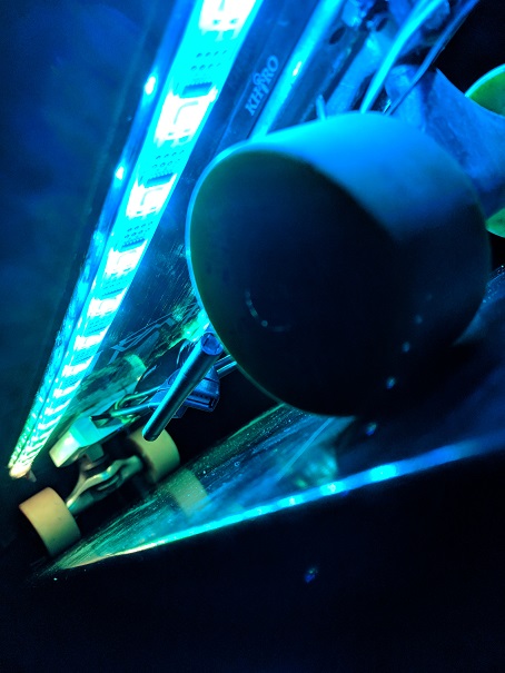
The project focuses on the idea manipulating an array of LEDs based on sound input. The array of LEDs could mimic a sound equalizer, change colors based on the sound intensity, beat, or frequency of the music. This project would be placed on a transportation tool such as a bike or skateboard simply for the aesthetics. A microphone would feed the analog data, and then be converted to digital via an ADC IC that outputs frequency bands. A PCB board will be used to power all LEDs, have a display terminal for user input features, and microphone connection. The data fed into the SJone board will then be filtered, processed, then sent to display onto the LEDs according to the music.
Team Members & Responsibilities
- Alan Chen
- LED Driver & sound behavior mechanics, code integration for LED Design
- Dhaval Raval
- PCB design, Hardware Design
- Sarvesh Harhare
- Audio Signal Processing
- Kathan Patel
- Data logging, IoT
- Audio Signal Processing
- Niraj Surti
- Availability of data collected over local network to be accessed by other modules.
Schedule
| Week# | Start Date | Planned Work | Actual Work | Progress |
|---|---|---|---|---|
| 1 | 4/10/18 | Project Job Discussion/Parts List | Project Division Discussion/Project Scope | Completed |
| 2 | 4/17/18 | WikiPage/PCB Design/Parts Ordered/Coding | Majority Parts Received/Drivers Written | Complete |
|
|
|||
| 3 | 4/24/18 | PCB Design/IoT/LED | PCB Design/Start IoT/Testing LED Drivers | Complete |
|
|
|||
| 4 | 5/1/18 | Implementation/Testing PCB/Coding | Ordered PCB/LED Behavior Modes/Debugging | Complete |
|
|
|||
| 5 | 5/8/18 | Testing/Debugging/Hardware Design | LED Mode Input/IoT Integration/Freq Analysis | Complete |
|
|
|||
| 6 | 5/15/18 | Debugging/Mounting/Finalizing | Mounting and Testing | Complete |
|
|
|||
| 7 | 5/22/18 | Final Exam/Writing Report |
|
Complete |
| 8 | 5/23/18 | Demo/Presentation |
|
Complete |
Parts List & Cost
| Part Name | Cost Unit Item | Qty | Comments |
|---|---|---|---|
| SJone Board | $80 | 3 | LED behavior & IoT hub (send & receive) |
| Skateboard | $40 | 1 | Project Mount |
| LEDs strips | $26.95 | 2 | 1 Meter RGB LED strips |
| PCB | $30 | 3 | One for each SJone Board |
| 3.5mm Jack | $7 | 1 | Receiver of Music |
| USB Type B Connector | $0.75 | 2 | Power Source for LED |
| MSGEQ7 | $4.95 | 1 | 7-Band Graphic Equalizer |
Design & Implementation
Hardware Design
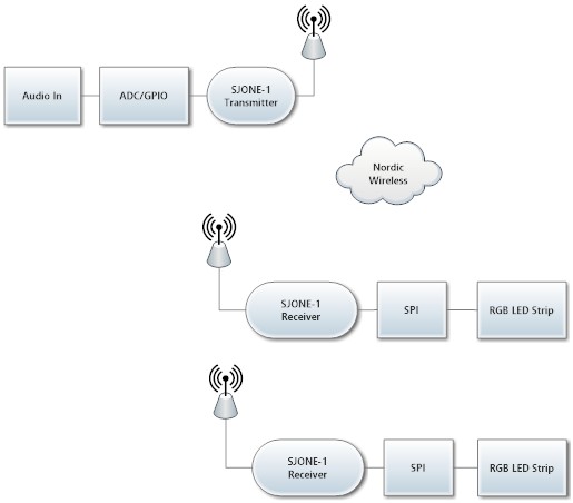
Hardware Configuration The block diagram and the connectivity of the hardware is shown in below block diagram of hardware.
The hardware is design in Altium Designer. PCB and Schematics were designed in Altium for our application. The Hardware has two main different part one is the audio input interface and other part is to provide power and SPI connectivity to the RGB LED strip. To design hardware in altium first we have to create a new project and inside new project we have to create new schematic documents in which we can design our circuit. Altium does not have the component libraries for every component which were used in the project. For that, we have to create a new library and create components schematic symbol and PCB footprint according to the datasheet. After designing the circuit in schematic we have to create new pcb document in the current project and change the size according to the estimation of the footprint.
Schematic Design
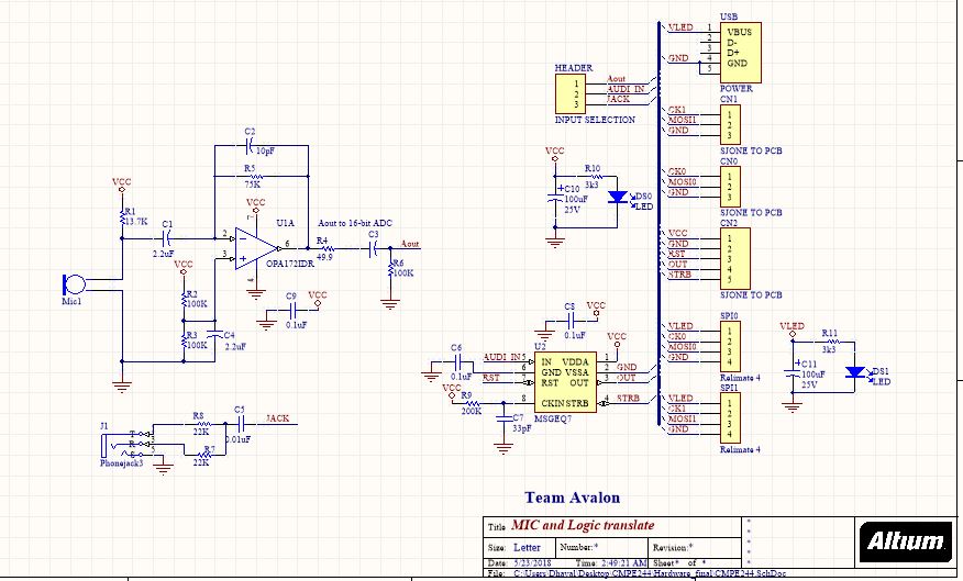
The schematic diagram below shows the circuit of the audio interface which can be fed via microphone or the 3.5mm audio input jack. The header is for selecting the audio input source either from Microphone or 3.5mm Jack. MSGEQ7 is used for filtering the audio input for 7 band. USB type B connector is for power connection for RGB LED strip as it consumes high power and we can not supply it from the SJONE boards.
PCB
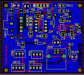
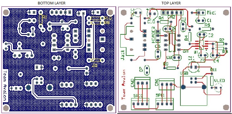
After creating the PCB document we just have import changes from schematic which will import every components in the pcb document with marked possible net connections. PCB size is 2.55 in x 2.275 in. The ground plane is placed on bottom layer for batter connectivity ground. Minimum trace width is 8 mils and maximum is 12 mils as we do not have high power traces.
Altium PCB View
PCB view of different Layer
Audio Analyzer
Introduction:
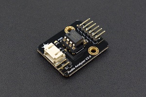
This Audio Analyzer module features the MSGEQ7 graphic equalizer display filter. Sound is broken down into seven frequency bands and the peak level for each band can be read. The seven frequencies measured are as follows: 63Hz, 160Hz, 400Hz, 1kHz, 2.5kHz, 6.25kHz and 16kHz. This Audio Analyzer module can be used to create sound visualizers, detect patterns in music or add sound activation to the microcontroller.
Description:
The seven band graphic equalizer IC is a CMOS chip that divides the audio spectrum into seven bands, 63Hz, 160Hz, 400Hz, 1kHz, 2.5kHz, 6.25kHz and 16kHz. The seven frequencies are peak detected and multiplexed to the output to provide a DC representation of the amplitude of each band. No external components are needed to select the filter responses. Only an off chip resistor and capacitor are needed to select the on chip clock oscillator frequency. The filter center frequencies track this frequency. Other than coupling and decoupling capacitors, no other external components are needed. The chip supply can be between 2.7 and 5.5 volts with 5 volts providing the best performance. The device has very low quiescent current (less than 1mA typical) for portable audio devices. The multiplexer is controlled by a reset and a strobe, permitting multiplexer readout with only two pins. The multiplexer readout rate also controls the decay time (10% decay per read), so no external pins are needed for this function.
Multiplexer Operation:
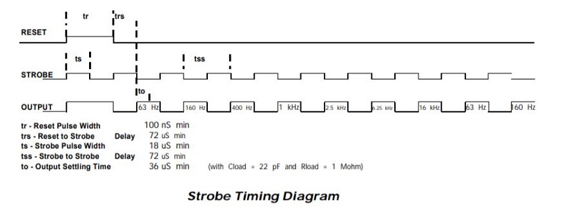
The DC peak output for measurement is selected using the reset and strobe pins. Reset high resets the multiplexer. Reset low enables the strobe pin. After the first strobe leading edge, 63Hz output is on OUT. Each additional strobe leading edge advances the multiplexer one channel (63Hz, 160Hz, 400Hz, 1kHz, 2.5kHz, 6.25kHz, 16kHz etc.) and this will repeat indefinitely. The multiplexer read rate is also the output decay time control. Each read decays that channel approximately 10%.
RGB LED Strips
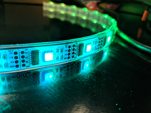
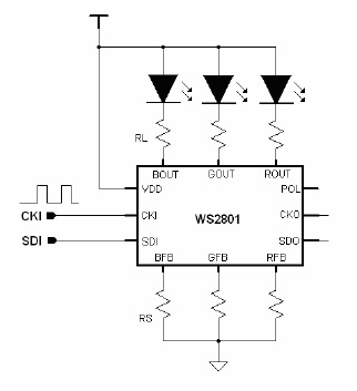
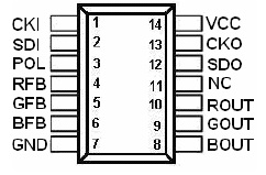
The WS2801 IC is a LED driver designed for RGB LED displays and lighting systems. In the project, the WS2801 is utilized in a cascading RGB LED strip. The WS2801 adopts a two-wire input control scheme, consisting of a data and clock input. The WS2801 will either output a PWM waveform (out of Bout, Gout, Rout) or send the data and clock to the following WS2081 using serial shift registers. In order to communicate and manipulate the RGB LED's, SPI is suggested in order to drive the clock and specified data waveform into the WS2801 (refer to software section). In order to latch the data fed into the WS2801, a 500 micro-second period (where the clock input is set low) is required in order shift the data into the next cascading WS2801. The following images below and table will give a diagram of the WS2081 pinout and basic circuit diagram of the LED strip. Since the WS2801 echos the data to the next WS2801, users will be able to address to each individual LED and set the color upon latch.
| Specifications | Min | Max | Units |
|---|---|---|---|
| Input Clock Freq | 25 | MHz | |
| Power Supply Volt | 3.3 | 5.5 | V |
| Latch Time | 500 | us | |
| Input Current | -1 | 1 | uA |
| Constant Output Current | 5 | 30 | mA |
| Output Pin Voltage | -0.3 | 7 | V |
| Power Dissipation | 600 | mW | |
Hardware Interface
General Purpose Input Output (GPIO)
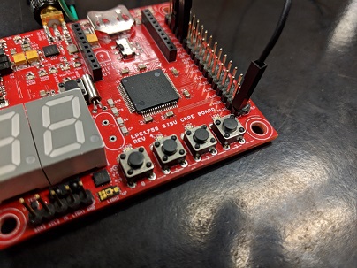
There are four switches (SW0-3) existing on the SJone board. Each switch is treated as an input pin. Each input pin symbolizes a feature for the LED strip (Mode, Color, Mode Behavior, Speed/Color Difference). In order to make sure the button was treated once for a single press, a basic de-bouncing check was done.
Serial Peripheral Interface (SPI)
The SJone board utilizes SPI in order to communicate to the WS2801 IC (RGB LED strip). In the datasheet, the WS2801 takes in a CLK and DATA (MOSI) Input from the SJone. The SJone board has two available SPI pins. However since SPI0 was utilized by the Nordic, SPI1 was the only SPI pin used to run a single LED strip consisting of 32 single bit RGB LEDs.
The micro-controller is connected to Nordic IC via SPI0 peripheral. Pins 15,16,17,18 of Port0 are SCK0 (clock), SSEL0 (Slave Select), MISO and MOSI respectively. A Hardware Interrupt flag (NORDIC_IRQ) is attached to Pin 22 of Port0, through an LED, as an External Interrupt.
Analog to Digital (ADC)
The Audio Analyzer has 4 main pins which are Left audio input, Strobe, Reset and Analog data out along with Vcc and Gnd. The Analog output goes to the 0.26 Pin of the SJOne board for analog to digital conversion whereas the Strobe and Reset are controlled by GPIO 0.0 and GPIO 0.1 respectively.
Software Design
SPI & Timer Counter (TC) Interrupts
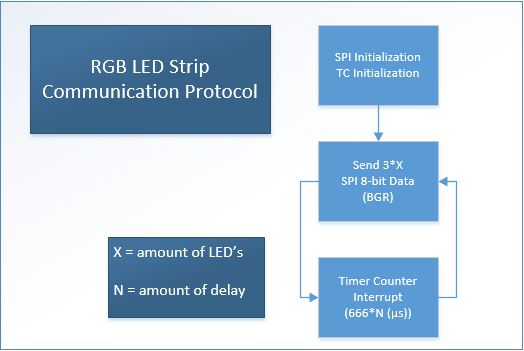
In order to send data to the RGB LED strips, certain timings and sequences must be sent and executed to change the LED strip behaviors. The SPI was used to communicate to the RGB LED Strip through 3 bytes of data that represent the Red, Green, and Blue 0-255 bit ratio. The Timing Interrupt was used in order to time a specified delay for the individually-address LEDs.
According to the WS2801 datasheet, a minimum of 500 micro-seconds is required to latch the data to the WS2801 IC. In order to create the exact timing, a timing interrupt of 666 micro-seconds was created to (frequency of 1500 Hz) triggers a flag that will allow a queue of SPI data to send to the RGB strips. Depending on the amount of LEDs, "N" amount of 3*8 bit RGB data will be sent to the RGB strip before setting a flag to latch the data to each individual strip.
When the SPI data is sent to the WS2801, the Blue data must be sent first instead of the Red data. This is due to the WS2801 interpretation of the RGB data. The WS2801 IC expect the least significant byte first to the most significant byte last (due to Endian interpretation).
Nordic RF Module
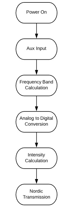
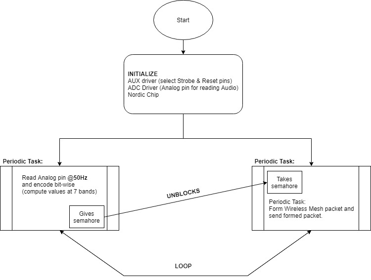
The communication between Audio Analyzer module and LED Display module is done utilizing the on-board Nordic IC. The analog data collected from audio equalizer chip is converted to digital format using ADC peripherals on the board. The data is then processed to determine speed, intensity and frequency range of operation before formatting and storing this data in a data structure. To decrease the payload size of packets, all the aforementioned properties of a band of frequency range are coded in one byte. Data of all the bands is then transmitted in a single packet. At the LED Display module, similar Nordic IC receives the data and extracts band information from the packet and sends to the task that is reponsible for changing the behavior of LEDs in the strip.
- Figure: Block diagram of Wireless communication
ADC Readings
LED Display
There are four modes, two behavior features, multiple selections of colors, and speed (refresh rate) in the LED display driver. Based on what was desired, specified algorithms were applied to create the behavior seen in the video and demo.
- Mode Selection
- Rain Mode - LED do a rain pattern as if moving a certain direction.
- Pulse Mode - Static LED colors pulse.
- Sound Mode - Changes color base on intensity of two bands.
- Equalizer Mode - Display four bands out of the seven on a single 32 bit RGB strip on four segments of 8 individual LEDs.
- Color Selection - select specified colors
- Behavior Selection
- LED Separation - select LED separation in rain mode
- Speed/Color Difference Selection - change speed and color difference
Implementation
This section includes implementation, but again, not the details, just the high level. For example, you can list the steps it takes to communicate over a sensor, or the steps needed to write a page of memory onto SPI Flash. You can include sub-sections for each of your component implementation.
RGB LED STRIP
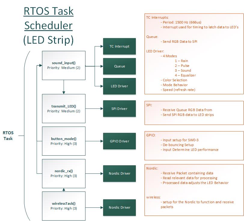
As show in the RGB LED Strip RTOS tasks, there are 5 tasks running. Each task have their own crucial responsibility in getting the project running with user capability.
Tasks:
- sound_input: PRIORITY MEDIUM
- This task requires a queue and selects which data will be sent to the RGB LED strip(s). All the processing and data/input selection is made here. This file requires the LED Driver library created by the team in order to get this task running functionally. This task also needs TC Interrupt Drivers in order to time when to send the queue at the exact moment (when the data from the individual LEDs latch).
- transmit_LED: PRIORITY MEDIUM
- The transmit_LED task is what sends the data, received from sound_input task, to the RGB LED Strip(s). The task requires the SPI drivers and is pretty simple.
- button_mode: PRIORITY HIGH
- Button_mode task checks for the input from the user from the SJone switches. In order to not register multiple times from a single press, a simple de-bouncing guard was created. Each switch represents a different feature on the board described on the software side. This task is purely for user configuration and behavioral choices.
- nordic_rx: PRIORITY HIGH
- The nordic_rx task is mainly to receive the data sent from the other SJone board transmitting the data (frequency bands and intensity). When sound or equalizer mode is set, the data packet is then interpreted and sent to the sound_input for processing.
- wirelessTask: PRIORITY MEDIUM
- The wirelessTask is the crucial task used to receive or send data when interfacing the Nordic. Without this, the wireless transmission portion would not work because the SPI0 drivers and other features were included in this task.
Nordic Wireless
At Transmitter Side:
- Obtain input from ADC and determine speed, intensity and band of frequency range.
- Form the payload with the data using correct destination address and an appropriate acknowledgement scheme.
- Send the formed packet.
At Receiver Side:
- Extract the band information from the received packet.
- Send the data in a queue for the LED task to receive and modify LED behavior.
Testing & Technical Challenges
Describe the challenges of your project. What advise would you give yourself or someone else if your project can be started from scratch again? Make a smooth transition to testing section and described what it took to test your project.
Include sub-sections that list out a problem and solution, such as:
<Bug/issue name>
Attaining 800 kHz on a PWM LED Strip
| Goal: | Achieve 800kHz PWM on a LED strip (WS2812B). |
| Issue: | Barely Reach 800kHz PWM using PWM Interrupt Driver and/or TC Interrupt Driver |
| Background | TBA |
| Conclusion: | Hardware can barely obtain ~800kHz waveform at the cost of RTOS performance and requires speed of a PLL CPU speed of 100MHz on SJone. Utilize Different LED strip and change protocol to SPI. |
Smooth transfer of data in the wireless network
| Goal: | Continually transfer data from over wireless channel with minimum delay. |
| Issue: |
|
| Background |
|
| Conclusion: | After fixing the aforementioned bugs, the communication was continuous and smooth. |
Conclusion
Conclude your project here. You can recap your testing and problems. You should address the "so what" part here to indicate what you ultimately learnt from this project. How has this project increased your knowledge?
Project Video
Upload a video of your project and post the link here.
Project Source Code
References
Acknowledgement
We would like to thank the CMPE244 Team and Professor Preetpal Kang for their
