S18: M.E.O.W
Contents
Microcontroller Energy Observation Widget (M.E.O.W)
Abstract
Our project aims to provide a theft detection service by recording a video when any movement is detected in an immediate vicinity. A video feed is stored on the device to collect later on. The video feed can be used as evidence to provide authority to find the culprit. This report details the system and technology used to implement this project.
Objectives & Introduction
Show list of your objectives. This section includes the high level details of your project. You can write about the various sensors or peripherals you used to get your project completed.
Our primary goal for this project was to learn about the sleep modes that the LPC Microcontoller is capable of. In order to help us understand the functionality of the technology, we wanted to implement the sleep modes on a real life practical example.
Living in the Bay Area, a highly technological society, most tech employees travel with expensive equipment in their cars. Knowing this thieves consider this a prime area to conduct car robberies. Recently there has been an increase in these car robberies, where it can be hard to catch the criminals who have committed the theft. Often times the robbers work so quickly and discretely that a normal bystander might not consider the act suspicious. Additionally if your car is parked in remote area, far away from city cameras, it can be hard gather any evidence to catch the thief. Video surveillance evidence is highly valuable to an investigator assigned on the case.
Our video surveillance device, records footage if a crime is committed in a customers' car. Sensors in our device activate a camera to start recording when movement is detected. In its idle state, the device is in sleep mode where minimal tasks are being run on the device, which means it saves on a lot of power consumption. Alternatively if the device is constantly polling, this would use up an enormous amount of battery power. Since this device is meant to be running in a car that is not running, it is pertinent to use minimal power unless absolutely necessary to maximize the battery life.
This application can be scaled for any environment; your home, backyard, or even for city use. We can connect it every street lamp with some IOT capabilities resulting in lower crime rate across the city.
Objectives:
- Research Power consumption capabilities of micro-controllers.
- Build and implement a video surveillance device to feature the low power methods.
Team Members & Responsibilities
- R "Meow Meow" Nikfar
- Team Lead, PCB Design, Sensor Design and Implementation, Hardware Testing, Power Analysis, Sleep-Mode Firmware
- Ahsan "Whiskers" Uddin
- BeagleBone Testing, Video Capture Implementation, Storage, Sleep-Mode Research
- Nelson "Fluffy" Wong
- Deep Power Modes, Power Analysis, Communications
- Britto "Kitty Kat" Thomas
- CAN BUS Low Power Research, Power Analysis, System Design
- Sai Kiran "Mittens" Rachamadugu
- Testing, Board Communications, User Interface
Schedule
| Week# | Date | Task | Status |
|---|---|---|---|
| 1 | 03/04 |
|
|
| 2 | 03/11 |
|
|
| 3 | 03/18 |
|
|
| 4 | 03/25 |
|
|
| 5 | 04/01 |
|
|
| 6 | 04/08 |
|
|
| 7 | 04/15 |
|
|
| 8 | 04/22 |
|
|
| 9 | 04/29 |
|
|
| 10 | 05/06 |
|
|
| 11 | 05/13 |
|
Parts List & Cost
Give a simple list of the cost of your project broken down by components. Do not write long stories here.
Design & Implementation
The design section can go over your hardware and software design. Organize this section using sub-sections that go over your design and implementation.
Hardware Design
Discuss your hardware design here. Show detailed schematics and the interface here.
GPIO Pins
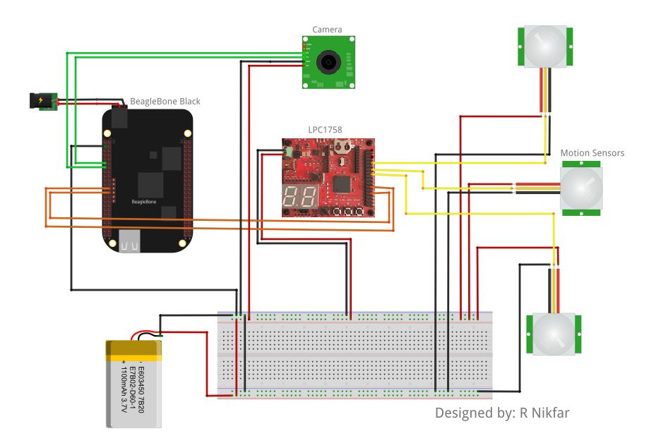
M.E.O.W uses three PIR sensors , each of these sensors are connected to GPIO pins on port 2.3 , 2.4 and 2.5. Any motion detected asserts these pins creating a WIC to wake up the system from sleep.
GPIO pin 1.28 is asserted to signal beagle bone to start recording.
Low-Level Hardware
The low-level design starts from the PIR Motion Sensors and ends with the storage of the video data. The LPC1758 plays a big role in the communication of the overall system. The PIR sensors are each connected to the LPC1758 using a GPIO protocol and send signals if an object or and person is within their range. Once the signal is sent from the Sensors, the LPC wakes up and consumes power from the PCB which either uses the power from a plugged source or the backup LIPO battery. LPC then sends the right information to the BeagleBone board using UART protocol.
Software Design
ADD description and design of the software for both the boards
freeRTOS Tasks
For this project, we use two RTOS tasks, one for asserting GPIO pin needed for beagle bone and the other to put the LPC board to sleep. The PIR task which asserts GPIO pin is given a higher priority compared to the task which puts the LPC board to sleep.
Psuedo-code
Void PIRTask (void* pvParams){
              while(1){
                 if(xSemaphoreTake(xGetSemfromISR,portMAX_DELAY){

                       // assert GPIO pin to signal beagle bone for recording video
                       LPC_GPIO1->FIOSET = 1 << “pin number”;
                }
        }
 }
Above code allows PIRTask to assert a GPIO pin to signal beagle bone to start recording. To put the LPC board to sleep a second task with lower priority is run. This task in-turn calls appropriate sleep mode.
Void PutToSleep(void* pvParams){
	While(1){
             if(xSemaphoreTake(xGetSemforSleep,portMax_DELAY){
                      //call appropriate sleep function
                       enter_powerdown();

             }
        }
  }
Interrupt request handler is created for above tasks which uses xSemaphoreGiveFromISR on interrupt to give a semaphore to the tasks. The code given below shows a pseudo-code for the Interrupt handler.
  void Simple_IRQHandler(){

        long yieldRequired = 0;
        xSemaphoreGiveFromISR(xGetSemfromISR, &yieldRequired);
        portYIELD_FROM_ISR(yieldRequired);

   }
Printed Circuit Board Design
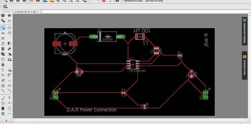
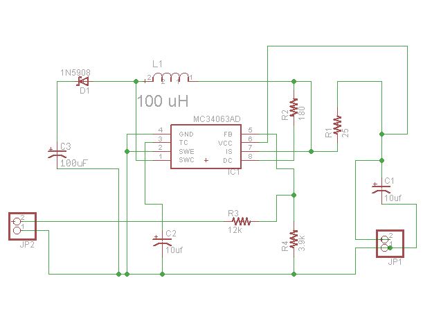
In order to stabilize and provide a noise free power supply to all the components of the system, a printed circuit board(PCB) was created. This piece of hardware brings all the power consumption of the unit together. The design and the creation of the board was done in Eagle Schematics Software where the gerber files were created. Once the gerber files were ready, the files were sent to be printed. There were 2 iteratins of this board. The first lacked the necessary connections for the additional components and had several noise reduction flaws. The second board solved all these issues. Note that the final board had to be 1 layer due to the noise reduction characteristics of the material and the ability for placement of the LIPO battery on the bottom of the board.
NXP LPC1700 Series Power Modes
Power management functionality in LPC 176x CPU
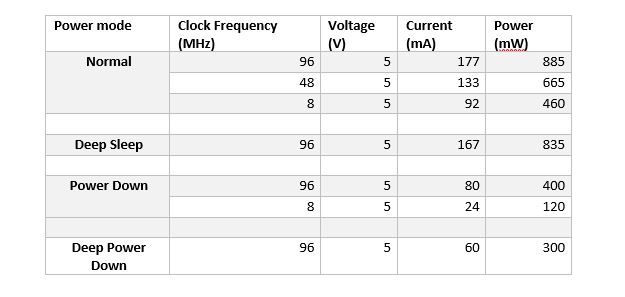
There are mainly 4 modes of runtime power savings mode that are available in LPC 176x CPU. They are described in details as follows. It should be noted that our SJ One board generally runs at 96MHz with 5V input voltage and consumes about 177mA of current which corresponds to 885mW of power.
Deep sleep
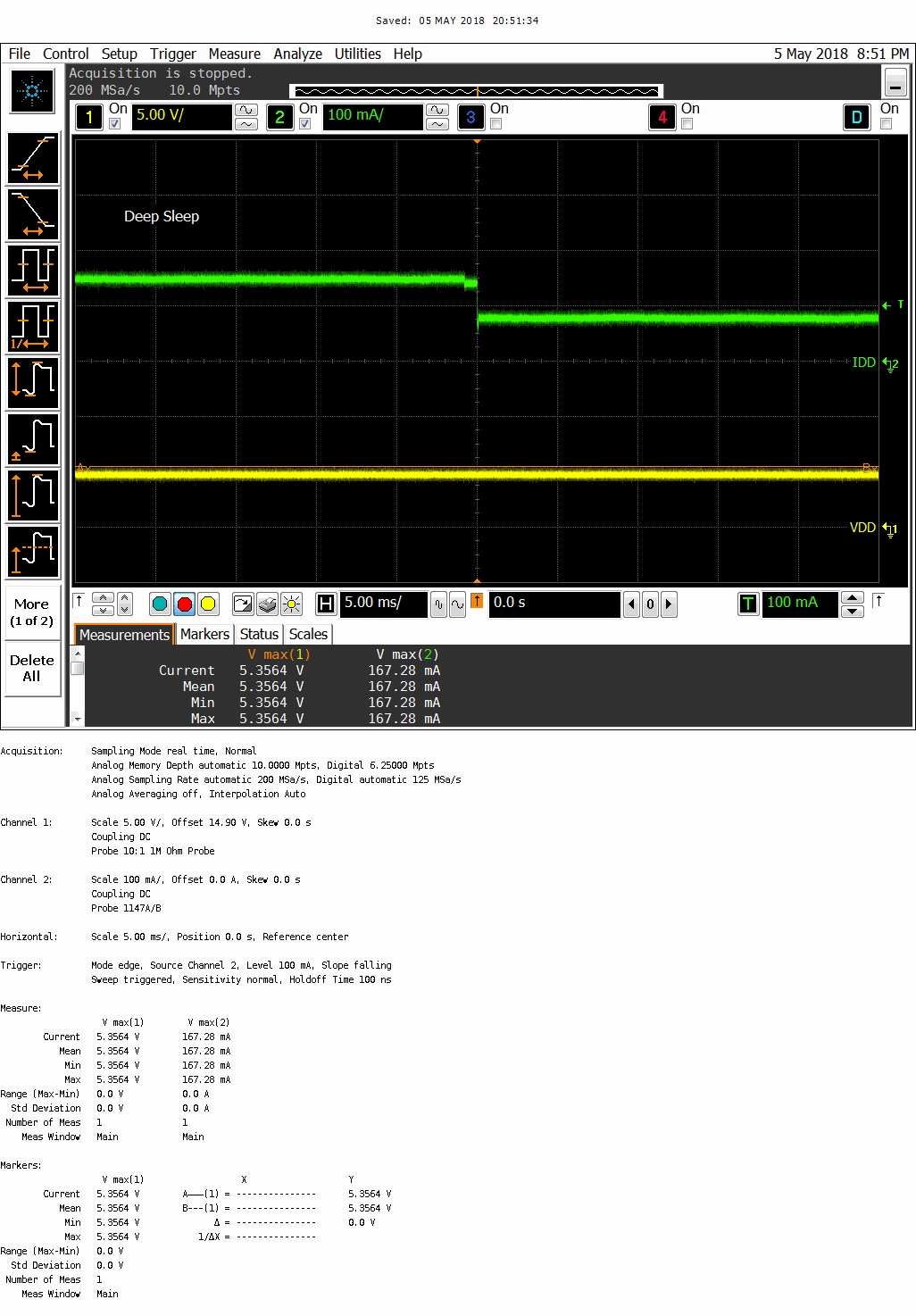
Upon entering the Deep sleep mode, the main oscillator is powered down and the DSFLAG in PCON is turned on. We observed that the current consumed at this state was 167mA which corresponds to 835mW of power. To wake up from Deep Sleep, an EINT0 was used to resume the CPU. Note that as PLLs are shut off during this sleep, the PLLs are configured once the CPU is resumed from deep sleep.
Power Down mode
Upon entering the Power Down mode, like deep sleep the main oscillator is powered down but additionally the flash is also turned off. We observed that the current consumed at this state was 80mA which corresponds to 400mW of power. To wake up from Deep Sleep, an EINT0 was used to resume the CPU. Note that as PLLs are shut off during this sleep, the PLLs are configured once the CPU is resumed from deep sleep.
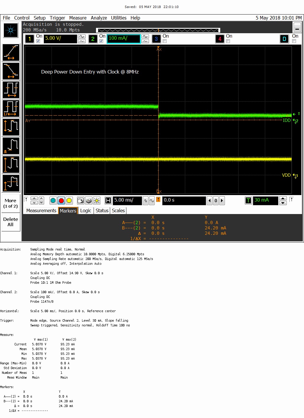
As we learnt in this semester that frequency plays a role in power consumption, and as we know that the default frequency of the LPC board is 96MHz, we tried the same power down sequence wit 8MHz. This time we saw that the current consumption went down to 24mA which corresponds to only 120mA!!! By far, this was the most stable power saving feature we have tested and we implemented this setting in our project.
Deep Power mode
Upon entering the deep power down mode, the entire chip is powered down except the RTC and the DPDFLAG in PCON is turned on. We observed that the current consumed at this state was 60mA which corresponds to 300mW of power. To wake up from Deep Sleep, there is only one way i.e to set the RESET pin, which replicates very closely to the cold boot process.
Summary of Power modes
Below is a chart for all the power savings comparisons side by side.
One things that needs to be noted is that although we are manipulating the power states we are still seeing a significant amount of current being drawn constantly. For example we are claiming that in deep power down, the ASIC is switched off but yet we see 60mA of current being drawn. The answer is that is even though the ASIC is switched off, there are other peripherals that are still ON. For example the 7 segment LED. So ideally it would be interesting to see what happens when each and every single peripheral is turned off dynamically in each state and to see the absolute power savings consumption.
Entering
Power mode entry is based on tables 44 (Power Mode Control register) and 662 (SCR bit assignments) of UM10360 [1].
void enter_sleep()
{
   LPC_SC->PCON = 0x0; // Table 44
   SCB->SCR     = 0x0; // Table 662
   __WFI();
}

void enter_deep_sleep()
{
    LPC_SC->PCON  = 0x8; // Table 44
    SCB->SCR     |= 0x4; // Table 662
    __WFI();
}

void enter_powerdown()
{
    LPC_SC->PCON  = 0x1; // Table 44
    SCB->SCR     |= 0x4; // Table 662
    __WFI();
}

void enter_deep_powerdown()
{
    LPC_SC->PCON  = 0x3; // Table 44
    SCB->SCR     |= 0x4; // Table 662
    __WFI();
}
Note the use of of __WFI(), which the compiler resolves as the assembly directive
__ASM ("wfi");
Exiting
On exiting a power mode, the associated bit on the Power Mode Control register must be cleared. As noted in the datasheet, bits 8, 9, 10, and 11 are associated to the particular power modes, and these flags are cleared in software by writing "one" to the associated bit.
void clear_sleep()          { LPC_SC->PCON |= 1 <<  8; };
void clear_deep_sleep()     { LPC_SC->PCON |= 1 <<  9; };
void clear_powerdown()      { LPC_SC->PCON |= 1 << 10; };
void clear_deep_powerdown() { LPC_SC->PCON |= 1 << 11; };
The PLLs (phase-locked loops) are turned off upon entering deep sleep, power-down, and deep power-down. Additionally, the IRC (the 4 MHz internal reference clock) and the clock dividers are reset when entering power-down and deep power-down. Therefore, the system clocks must be reconfigured/reinitialized when exiting any of these power modes.
We can take advantage of sys_clock_configure() from L0_LowLevel/sys_clock.cpp to perform this initialization.
One more thing to keep in mind regarding power mode exits: when exiting deep sleep, power-down, and deep power-down, there is a non-zero amount of time that must elapse before the system is able to resume processing. In all three cases, a timer starts counting the moment the power mode is exited, and code execution can resume after this timer expires.
- If the IRC was used prior to entering the power mode, then the 2-bit IRC timer is used, and it lasts is 22 = 4 cycles long.
- If the main external oscillator was used, then the 12-bit main oscillator timer is used, and it lasts 212 = 4096 cycles long.
Moreover, in power-down and deep power-down, the flash undergoes wake-up, and its wake-up timer must expire (approximately 100 µs) before it can be used. This means that no instructions can be fetched from flash for execution until this timer expires.
Below is a tabulation of the features that are enabled or disabled for each power mode.
| Features | Sleep | Deep-sleep | Power-down | Deep Power-down |
|---|---|---|---|---|
| Wake via reset | Yes | Yes | Yes | Yes |
| Wake via RTC interrupt | Yes | Yes | Yes | Yes |
| Wake via NMI | Yes | Yes | Yes | No |
| Wake via EINT0-3 | Yes | Yes | Yes | No |
| Wake via GPIO interrupts | Yes | Yes | Yes | No |
| Wake via Eth WOL interrupt | Yes | Yes | Yes | No |
| Wake via brownout detect | Yes | Yes | Yes | No |
| Wake via watchdog timer | Yes | Yes | Yes | No |
| Wake via USB-active interrupt | Yes | Yes | Yes | No |
| Wake via CAN-active interrupt | Yes | Yes | Yes | No |
| Wake via any other interrupt | Yes | No | No | No |
| Main oscillator? | Enabled | Disabled | Disabled | Disabled |
| IRC oscillator? | Enabled | Enabled | Disabled | Disabled |
| RTC oscillator? | Enabled | Enabled | Enabled | Optional |
| CPU clock? | Disabled | Disabled | Disabled | Disabled |
| Peripheral clocks? | Enabled | Enabled | Disabled | Disabled |
| USB clock? | Enabled | Disabled | Disabled | Disabled |
| Watchdog clock? | Enabled | Enabled | Enabled* | Disabled |
| PLLs? | Enabled | Disabled | Disabled | Disabled |
| Status of Wake-up Interrupt Controller? | Active | Active | Active | Active |
| Status of RTC backup registers? | Active | Active | Active | Active |
| Status of on-chip regulator? | Active | Active | Active | Active or power-down with external circuitry |
| Status of flash memory? | Standby | Standby | Powered-down | Powered-down |
| Status of processor state? | Preserved | Preserved | Preserved | Powered-down |
| Status of processor registers? | Preserved | Preserved | Preserved | Powered-down |
| Status of peripheral registers? | Preserved | Preserved | Preserved | Powered-down |
| Status of SRAM values? | Preserved | Preserved | Preserved | Powered-down |
| Status of chip pin logic levels? | Preserved | Preserved | Preserved | Powered-down |
| Access to flash memory? | Disabled | Disabled | Disabled | Disabled |
| Access to main SRAM? | Disabled | Disabled | Disabled | Disabled |
| Access to AHB SRAM? | Allowed with GPDMA support | Allowed with GPDMA support | Disabled | Disabled |
| Access to peripherals? | Allowed with GPDMA support | Allowed with GPDMA support | Disabled | Disabled |
| Dynamic power? | Disabled | Disabled | Disabled | Disabled |
| Special instructions after wakeup? | No | Yes | Yes | Yes |
| Resume from last PC? | Yes | Yes | Yes | No; system restarts |
Hardware Interface
In this section, you can describe how your hardware communicates, such as which BUSes used. You can discuss your driver implementation here, such that the Software Design section is isolated to talk about high level workings rather than inner working of your project.
Software Design
Show your software design. For example, if you are designing an MP3 Player, show the tasks that you are using, and what they are doing at a high level. Do not show the details of the code. For example, do not show exact code, but you may show psuedocode and fragments of code. Keep in mind that you are showing DESIGN of your software, not the inner workings of it.
Implementation
This section includes implementation, but again, not the details, just the high level. For example, you can list the steps it takes to communicate over a sensor, or the steps needed to write a page of memory onto SPI Flash. You can include sub-sections for each of your component implementation.
Testing & Technical Challenges
Describe the challenges of your project. What advise would you give yourself or someone else if your project can be started from scratch again? Make a smooth transition to testing section and described what it took to test your project.
Include sub-sections that list out a problem and solution, such as:
<Bug/issue name>
Discuss the issue and resolution.
Conclusion
Conclude your project here. You can recap your testing and problems. You should address the "so what" part here to indicate what you ultimately learnt from this project. How has this project increased your knowledge?
Project Video
Upload a video of your project and post the link here.
Project Source Code
References
Acknowledgement
Any acknowledgement that you may wish to provide can be included here.
References Used
List any references used in project.
[1] NXP Semiconductors. (19 Dec. 2016). UM10360: LPC176x/5x user manual.
[2] NXP Semiconductors. (25 Feb. 2010). AN10915: Using the LPC1700 power modes.
Appendix
You can list the references you used.
