S15: RFID Security Box
Contents
Grading Criteria
- How well is Software & Hardware Design described?
- How well can this report be used to reproduce this projec
- Code Quality
- Overall Report Quality:
- Software Block Diagrams
- Hardware Block Diagrams
- Schematic Quality
- Quality of technical challenges and solutions adopted.
Project Title
Abstract
The RFID Security Box is a container with an electronic lock that can be unlocked by using RFID tags, NFC-compatible devices, or a manually entered passcode.
Objectives & Introduction
Show list of your objectives. This section includes the high level details of your project. You can write about the various sensors or peripherals you used to get your project completed.
A security box for storing valuables that is accessible through a numeric keypad, NFC-compatible device, and RFID tags, tokens, and cards.
- NFC/RFID Controller breakout board
- Lock-style Solenoid
- 3x4 Phone-style Matrix Keypad
- RGB LCD Screen
Team Members & Responsibilities
- Rajwinder Ruprai
- NFC/RFID driver
- Sofwtare testing
- Charles MacDonald
- Hardware and software design
- Physical construction
- Hardware testing
Schedule
Show a simple table or figures that show your scheduled as planned before you started working on the project. Then in another table column, write down the actual schedule so that readers can see the planned vs. actual goals. The point of the schedule is for readers to assess how to pace themselves if they are doing a similar project.
| Week# | Date | Task | Actual |
|---|---|---|---|
| 1 | 04/14 | Order parts needed for required functionality, work on box design (component placement, mounting requirements, etc.) |
Completed |
| Week# | Date | Task | Actual |
|---|---|---|---|
| 2 | 04/21 | Develop keypad and LCD display drivers. | In progress |
| Week# | Date | Task | Actual |
|---|---|---|---|
| 3 | 04/28 | Develop solenoid driver and start work on RFID/NFC driver. | Finished. |
| Week# | Date | Task | Actual |
|---|---|---|---|
| 4 | 05/5 | Finish RFID/NFC driver, finish PSU wiring. | Finished. |
| Week# | Date | Task | Actual |
|---|---|---|---|
| 5 | 05/12 | Component integration and testing. | Finished. |
| Week# | Date | Task | Actual |
|---|---|---|---|
| 6 | 05/19 | Tweaking and polishing implementation. | Finished. |
| Week# | Date | Task | Actual |
|---|---|---|---|
| 7 | 05/25 | Project presentation. | Rescheduled. |
Parts List & Cost
Give a simple list of the cost of your project broken down by components. Do not write long stories here.
| Quantity | Description | Cost |
|---|---|---|
| 1 | Lock-style Solenoid - 12VDC | $14.95 |
| 1 | I2C / SPI character LCD backpack (not used) | $10.00 |
| 1 | MiFare Classic (13.56 MHz) tag assortment (1KB) | $10.00 |
| 1 | PN532 NFC/RFID controller breakout board (v1.6) | $39.95 |
| 1 | 3x4 Phone-style Matrix Keypad | $7.50 |
| 1 | RGB backlight negative LCD 16x2 + extras (RGB on black) | $13.95 |
| 1 | Extra-long break-away 0.1" 16-pin strip male header (5 pieces) | $3.00 |
| 1 | Murata OKI-78SR Fixed Output 1.5A DC/DC Converter (5.0V) | $4.30 |
| 1 | ST Microelectronics 3.3V Linear Regulator (not used) | $0.64 |
| 1 | 1N4007 Diode | $0.13 |
| 1 | Meanwell RS-15-12 +12V, 1.3A PSU (not used) | $9.95 |
| 1 | IEC 320-C14 AC power receptacle (not used) | $0.79 |
| 1 | Ikea VALJE Wall Cabinet with Door | $35.00 |
Design & Implementation
The design section can go over your hardware and software design. Organize this section using sub-sections that go over your design and implementation.
Hardware Design
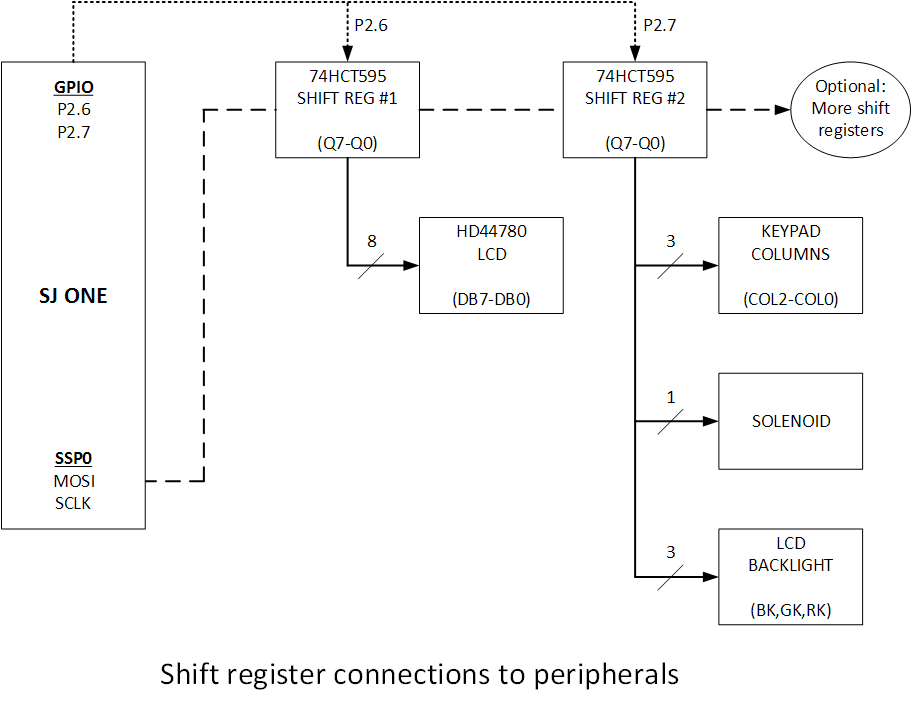
Initial rough draft of system architecture / schematic diagram (external link):
Hardware Interface
The various buses are allocated as follows
- UART2 (free)
- UART3 (free, either one is a candidate for the UART interface of the fingerprint reader)
- SSP0 Shift register chain
- SSP1 AT45/SD card/PN532
- GPIO Various control outputs and inputs
GPIO assignments
- P2.0 : Keypad matrix row data, bit 0
- P2.1 : Keypad matrix row data, bit 1
- P2.2 : Keypad matrix row data, bit 2
- P2.3 : Keypad matrix row data, bit 3
- P2.4 : Storage register clock for shift register #1
- P2.5 : Storage register clock for shift register #2
- P2.6 : External reset button input
- P2.7 : LCD interface, data bit 7 (input to read busy status)
- P0.19 : PN532 chip select for SSP1 bus (also shared with AT45 and SD card)
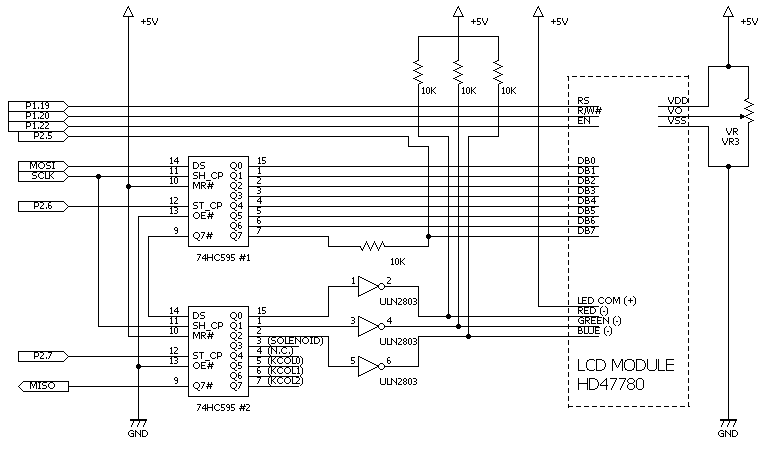
Shift register assignments
- S1.0 : LCD panel tri-color backlight LED blue cathode
- S1.1 : LCD panel tri-color backlight LED green cathode
- S1.2 : LCD panel tri-color backlight LED red cathode
- S1.3 : To solenoid coil connector
- S1.4 : Piezo buzzer (negative terminal)
- S1.5 : Keypad matrix column select, bit 0
- S1.6 : Keypad matrix column select, bit 1
- S1.7 : Keypad matrix column select, bit 2
- S2.0 : LCD interface, register select (RS)
- S2.1 : LCD interface, read/write (R/W#)
- S2.2 : LCD interface, enable strobe (EN)
- S2.3 : (Not used)
- S2.4 : LCD interface, data bit 4
- S2.5 : LCD interface, data bit 5
- S2.6 : LCD interface, data bit 6
- S2.7 : LCD interface, data bit 7
Keypad implementation
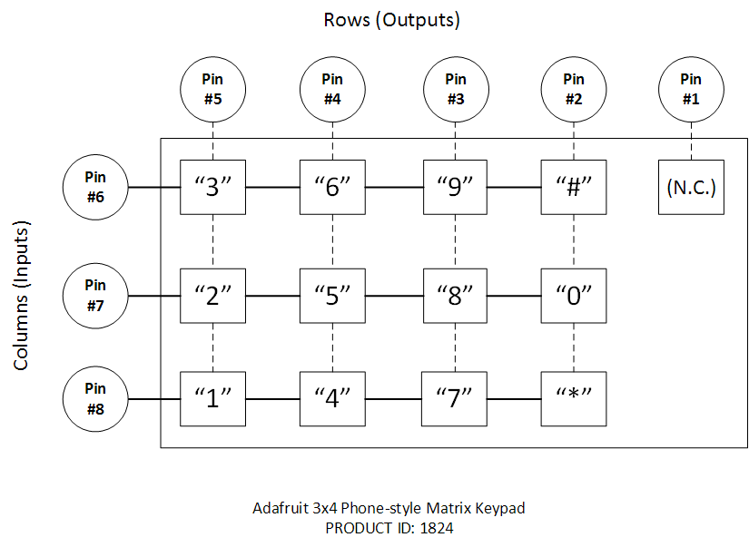
The keypad is arranged as a 4x3 matrix. Where each row and column intersect is a switch, and a physical connection between the row and column is made when the switch is depressed. Otherwise there is no connection when a switch is released, and the relationship between the row and the column at that point appears as an open circuit.
As the keypad has no datasheet the first task was to disassemble the keypad and use the continuity test function of a multimeter to determine the pin assignments:
- Pin 1 - Not used (goes to a test point on the PCB)
- Pin 2 - Row (keys *,0,#)
- Pin 3 - Row (keys 7,8,9)
- Pin 4 - Row (keys 4,5,6)
- Pin 5 - Row (keys 1,2,3)
- Pin 6 - Column (keys 3,6,9,#)
- Pin 7 - Column (keys 2,5,8,0)
- Pin 8 - Column (keys 1,4,7,*)
The notation of row vs. column is completely arbitrary, and were chosen only to have a consistent naming scheme.
Here is a diagram of the matrix inside the keypad:
LCD implementation
Solenoid implementation
The solenoid used (Adafruit #1512) is designed to function similarly to the latch of a door. A spring pushes the latch outwards such that the door is locked when the system is turned off. The solenoid contains a coil that generates a magnetic field when energized, which draws the latch inwards allowing the door to be opened. Thus the solenoid locks the door when off, and unlocks it when on.
The solenoid requires +12V to operate and draws 680mA normally. When the solenoid is turned off after a period of activation, the magnetic field collapses, at which point the force of the internal spring overcomes the force of the magnetic field holding the latch in place, and the spring can then move the latch to the outward position.
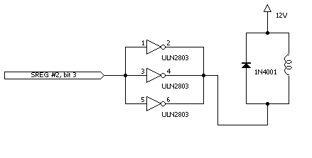
When the magnetic field collapses current is induced in the coil, causing a large voltage spike that can be damaging to any digital circuitry connected to it. To prevent this, a diode is placed in parallel with the solenoid coil with the cathode to the positive voltage supply (+12V). This provides a safe discharge path so that the voltage spike does not go into the digital circuitry.
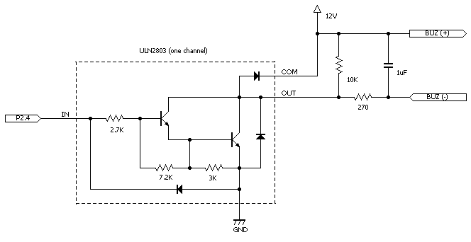
To control the the solenoid with a GPIO port, a ULN2803 is used, which is an eight channel Darlington transistor array. A Darlington transistor is a pair of transistors in series that can sink a large amount of current, and can interface to higher voltage signals such as 12V. The ULN2803 has built-in resistors to provide a TTL/CMOS compatible interface. Two important aspects to remember are the the Darlington transistors have an inverted output in relation to the input, such that an active-high input sinks current and an active-low input makes the output high impedance. Secondly, the high impedance output should have a pull-up or pull-down resistor to prevent the output from oscillating.
Adafruit sells the solenoid with the latch oriented in 90 degrees from the desired position. To correct this, the housing can be lifted up after removing two screws. There is a thin D-ring around the base of the latch which is quite hard to remove. Using a flat screwdriver head to push on one side of the ring while holding the other side in place with needlenose pliers worked eventually. There may be some kind of dedicated tool for D-ring removal which would simplify this process.
Keypad scanning
The keypad can be scanned as follows
1. Assign the columns as outputs (3-bit output). 2. Assign the rows as inputs (4-bit input), with internal pull-up resistors enabled. 3. For each column, drive the corresponding column output low (e.g. for column bits 2,1,0, the will be set to
- 1,1,0 : Select column #0
- 1,0,1 : Select column #1
- 0,1,1 : Select column #2
4. When a given column is selected, input the row data. 5. Row bits will be 0 where the row and column intersect AND the key is pressed, or 1 where the key is released.
Note that the keypad operation is fully mechanical like any switch, there is no ground or power connections necessary.
Piezo buzzer
The piezo buzzer is a thin plate that deflects when voltage is applied to it. This deflection is enough to create audible sound, and the plate is mounted in a plastic cavity for amplification. The buzzer can be controlled by DC voltage such that a square-wave of a given frequency, such as 440 Hz, creates a 440 Hz tone. At very low frequencies the buzzer can be used to make simple clicking sounds, such as to augment the keypad entry with clicks as each key is pressed. This kind of feedback makes it easier for the operator to tell if a key press was complete or not.
A 0.1uF ceramic disc capacitor is placed across the buzzer terminals to filter out high frequency noise, and a 270-ohm resistor is placed in series between the negative terminal to the Darlington transistor driving it to limit current -- not because the buzzer needs it, but because the piezoelectric effect means deflection on the plate can produce voltage going back into the transistor array, potentially causing damage.
When GPIO port P2.4 drives low, the corresponding ULN2803 output becomes high impedance, leaving the negative terminal of the buzzer floating. This makes it susceptible to noise which can be heard as audible clicks. A 10K pull-up resistor to +12V biases the negative terminal high, such that the voltage difference between both terminals is zero, thus the buzzer is in an idle state and will not oscillate.
Software Design
Show your software design. For example, if you are designing an MP3 Player, show the tasks that you are using, and what they are doing at a high level. Do not show the details of the code. For example, do not show exact code, but you may show psuedocode and fragments of code. Keep in mind that you are showing DESIGN of your software, not the inner workings of it.
Implementation
This section includes implementation, but again, not the details, just the high level. For example, you can list the steps it takes to communicate over a sensor, or the steps needed to write a page of memory onto SPI Flash. You can include sub-sections for each of your component implementation.
Shift register abstraction
The shift registers are abstracted as a chain of shift registers placed in series. The "sreg" class is used to get the state of a shift register (the last value written to it), and set the new state as well. The shift register update function actually updates the shift register chain with the new values.
This allows the shift registers to be expanded to any length up to 256 devices.
Queues and events
When the user enters data on the keypad this creates a key event. The key event stores the current keypad state and indications of what has changed, such as if a key was pressed or released. Key events are placed into the key queue for other tasks to retrieve user input.
Likewise an add_tone() function adds tone events to the tone queue. This is used to play back beeps that are generated when the user presses buttons on the keypad.
For the most part the tone and key events are tightly coupled, but the system was designed so that other sources could generate tones, such as RFID card swipe results which are independent of any key input.
User interface
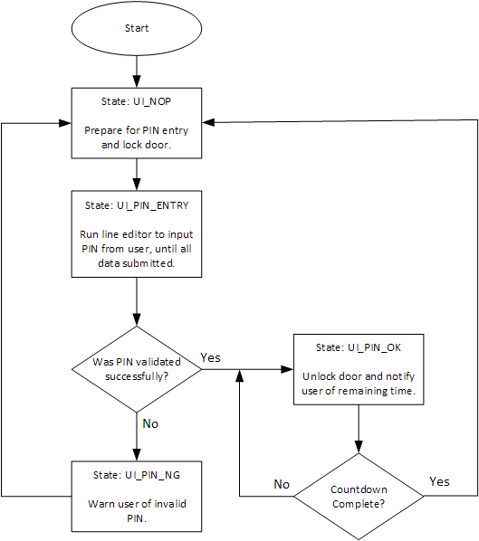
A line editor module was developed to allow complex data entry. It support commands such as delete (backspace), cancel, and submit. Certain keys can be restricted from input if desired. Various aspects of the editor are indicated in a status code, such that unique actions (playing tones, printing warning messages, etc.) can be carried out if the user makes actions such as:
- Overwriting existing text (overflow)
- Deleting non-existent text (underflow)
- Entering unacceptable keys
- Trying to submit incomplete data
The line editor can be expanded to work with larger keypads or even a full keyboard.
LCD display
The LCD display class provides a set of familiar functions for text output:
- clrscr() - Clear the display.
- gotoxy() - Set the cursor position.
- putch() and puts() - Print characters and formatted strings.
There are additional functions to control the blinking cursor as well.
Tasks
The main application creates three tasks:
1. Keypad scanning task. Low priority.
2. Finite state machine task. Low priority.
3. Buzzer update task. High priority.
Generates a square wave to the piezo buzzer by toggling the state every 1 microsecond. A complete square wave is produced in 2 microseconds, giving a 500 Hz tone.
Testing & Technical Challenges
Describe the challenges of your project. What advise would you give yourself or someone else if your project can be started from scratch again? Make a smooth transition to testing section and described what it took to test your project.
Include sub-sections that list out a problem and solution, such as:
Issue #1 : Backlight control
The LCD panel has a RGB backlight consisting of a single RGB LED, that has a common anode and three independent cathodes. Each cathode has a 200-ohm resistor in series to limit current to 25mA (when +5V supplied to the anode) per LED. In order to control the red, green, and blue channels of the backlight independently, a circuit is required that can interface GPIOs from the SJOne board to the cathode such that 25mA can be sunk per cathode. This amount of current to sink in order to fully turn on a single LED is beyond the limit of the LPC1758 ability, so a direct connection is not possible.
The solution is to use a Darlington transistor. The ULN2803 contains eight independent Darlington transistors, each of which has the appropriate base and collector resistors to appear as TTL/CMOS compatible inputs, suitable for control by the SJOne GPIOs directly. This chip can sink 500mA per transistor which meets and exceeds the current requirements of the RGB backlight.
Interfacing the backlight controls to three GPIOs will provide 2^3=8 total colors. However we will use the PWM function of the LPC1758 to to increase the range of available colors to several hundred thousand. This will also allow software-defined brightness control, to either set the brightness to a user-defined level or for strobing or flashing effects on the display by modulating the brightness over time.
Issue #2 : Power supply
The solenoid requires 12V, the SJOne board uses 3.3V, and the LCD backlight requires 5V. In order to meet this requirement a power supply circuit was designed with the goal of keeping efficiency high and heat output low.
A switching PSU is used to convert 120V AC to 12V DC for the solenoid. The 12V is fed into a switching 5V regulator to provide 5V for the LCD backlight. Note that the relatively large voltage drop from 12V to 5V does not cause excessive heat due to the switching regulator being used, thus no heatsinking or other cooling methods are required. Finally, the 5V is fed into a 3.3V linear regulator. At this point the voltage drop is relatively small (approx. 2V) and the corresponding heat dissipation is low.
In this way all three power rails (3.3V, 5V, and 12V) can be provided to the system. The least efficient part is the 3.3V linear regulator, but the switching 5V regulator and switching 12V PSU are highly efficient in terms of conversion.
Conclusion
Conclude your project here. You can recap your testing and problems. You should address the "so what" part here to indicate what you ultimately learnt from this project. How has this project increased your knowledge?
Future work
There are a number of ways to improve the project.
- Use PWM or a timer interrupt to control buzzer updates. This would allow for the frequency to be varied, allowing for frequency envelopes and sweeps, and more complex sound effects generated by linking single tone structures together.
- Use a 16x4 LCD display to display larger messages. The current 16x2 LCD is cramped, but functional.
- Use PWM to control the RGB LCD backlight cathodes. The current implementation wires these to the shift register, but if using three of the PWM channels the backlight colors could be expanded from eight to several million.
- Use a SPI GPIO expander. In particular the Microchip MCP23S17 has two 8-bit I/O ports that could have replaced the two 745HC595 shift registers. Note that the MCP23* line of GPIO expanders have rather unusual characteristics for their inputs regarding the Vil/Vih levels, so care must be taken when using their pins configured as inputs. However as outputs they function as expected.
- Use a different RFID chip other than the PN538.
- Support manual registration and management of PINs, either by using the internal operator button (more secure) or a dedicated service mode PIN (less secure).
In terms of physical security the solenoid can be triggered simply by applying +12V across the terminals with the control box disconnected. A more secure method would be to place a second SJ-One board inside the security box along with a dedicated power supply, and have the control box communicate to it over a serial link. The SJ-One in the security box can authenticate door open requests from the control box. The serial link could be protected by having data encrypted using a LFSR with a known seed shared between both systems which would make eavesdropping challenging, but would not stop a replay attack.
A further exercise in security would be to use a wireless system (XBee) for the control box and security box to communicate.
Project Video
Upload a video of your project and post the link here.
Project Source Code
References
Acknowledgement
Any acknowledgement that you may wish to provide can be included here.
References Used
List any references used in project.
Appendix
You can list the references you used.
