S16: Simpsons
Contents
- 1 Grading Criteria
- 2 Smart Walking Cane for Blind
- 3 Abstract
- 4 Objectives & Introduction
- 5 Schedule
- 6 Parts List & Cost
- 7 Design & Implementation
- 8 Conclusion
- 9 References
Grading Criteria
- How well is Software & Hardware Design described?
- How well can this report be used to reproduce this project?
- Code Quality
- Overall Report Quality:
- Software Block Diagrams
- Hardware Block Diagrams
- Schematic Quality
- Quality of technical challenges and solutions adopted.
Smart Walking Cane for Blind
Abstract
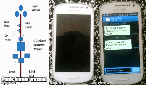
We are proposing an IoT device that helps the blind. We have developed a blind stick which provides vibration feedback on getting any information about the obstacles around the stick. Such a device would help a lot of blind people who need obstacle assistance in daily life. This device would include some ultrasonic obstacle sensors and a laser sensor to ignore the ground as an obstacle. The handle of the stick would provide a vibration feedback if it detects any obstacle. This feedback would not be a simple feedback. There would be vibrators installed on three sides of the handle. If the stick detects an obstacle on the left side, the stick handle would vibrate from the left side and similarly for the center and right side. This would help the user to react to these situation properly. Apart from this major feature, we have proposed two important features. One of which is a key locator and the other is an automatic messaging system. The key locator would help the blind person to find the bunch of keys wherever they are in the house. The other feature is an automatic messaging system which would send a message when a panic button is pressed. This button would be pressed when the user feels there is some kind of danger and need to send a message to close people.
Objectives & Introduction
Show list of your objectives. This section includes the high level details of your project. You can write about the various sensors or peripherals you used to get your project completed.
Team Members & Responsibilities
- Akshay Kanchar
- Key Locator
- Hardware
- Arvind Allawadi
- GSM module
- Bhushan Muthiyan
- Haptic feedback
- Treasurer
- Gaurao Chaudhari
- Sensor Interfacing and Algorithm
- Hardware and PCB designing
- Keerthana Alugudurai
- Haptic feedback
Schedule
| Sl. No | Start Date | End Date | Task | Status | Actual Completion Date |
|---|---|---|---|---|---|
| 1 | 04/05/2016 | 04/12/2016 | 1) Buying of blind stick and other important components 2) Development and Design of Software and Hardware Architecture |
Completed | 04/11/2016 |
| 2 | 04/12/2016 | 04/19/2016 | 1) Interfacing Sensors,Vibrators,Buttons and GSM with SJ One Board 2)Developing basic functionalities for Sensors and Vibrators |
Completed | 04/20/2016 |
| 3 | 04/19/2016 | 04/26/2016 | 1) Interfacing,implementation and integration of GSM module 2) Implementation of Key Locator functionality |
Completed | 04/28/2016 |
| 4 | 04/26/2016 | 05/03/2016 | Completing Integration of all modules and testing basic obstacle avoidance and haptic feedback | Completed | 05/05/2016 |
| 5 | 05/03/2016 | 05/10/2016 | Testing and resolution of Problems | Completed | 05/12/2016 |
| 6 | 05/10/2016 | 05/17/2016 | Final testing | Completed | 05/19/2016 |
Parts List & Cost
| Sr. No | Part Name | Source of Purchase | Part Number | Quantity | Cost($) |
|---|---|---|---|---|---|
| 1 | SJOne Board | Preet | 2 | $80 | |
| 2 | PCB | Designed by Self, Delivered by OSH Park | 1 | $35 | |
| 3 | Haptic Motor Driver | digikey.com | drv2605L | 3 | $4.79 |
| 4 | Haptic Vibrator | precisionmicrodrives.com | C10-100 | 5 | $9.41 |
| 5 | Ultrasonic Sensors | Amazon.com | HC-SR04 | 5 | $10 |
| 6 | 5V Battery | Self | 1 | $0 | |
| 7 | Velleman Economic DC Buzzer | Fry's Electronics | 7726668 | 1 | $2.99 |
| 8 | 2.4GHz Duck Antenna RP-SMA | sparkfun.com | WRL-00145 | 2 | $15.9 |
| 9 | GSM Module | Amazon.com | SIM900 | 1 | $30 |
| Total = | $371.21 |
Design & Implementation
PCB Design
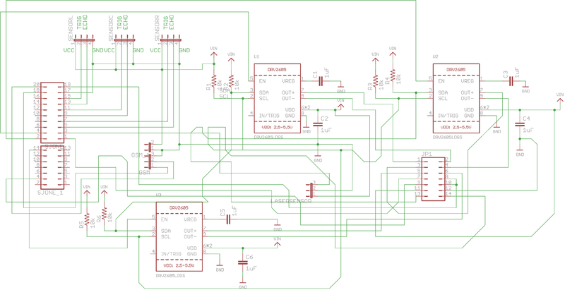
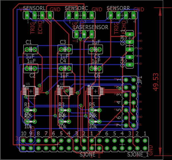
As we went ahead with the development of the hardware of system, the hardware was becoming more complex and then we decided that we need to design a PCB and order it. This way we were able to accommodate all the modules using the single PCB. The PCB made it much more easy to interface different peripherals and make it work. We have used PCB for all the modules our project. The sensors has its connection and the key locator, GSM module have jumpers to be connected to the PCB.
PCB Design Description
Following are the different modules to be connected to the PCB.
1) Ultrasonic Sensor
2) Laser Sensor
3) Haptic Vibrator motors
4) GSm Module
5) Key locator Buttons
6) Panic Message Buttons
PCB Schematic
PCB Board
Sensor Obstacle avoidance
When a blind person travels along the path, there can be a lot of obstacles on his/her way. One of the ways to avoid those obstacles is the ultrasonic sensor obstacle avoidance. These ultrasonic sensors detects obstacles in its 250 cms of distance. This distance varies depending on the make of the sensors. The sensors which we are using are HC-SR04 and the largest distance they can detect is 250 cms. There are other sensor manufacturers also which detect distances which are much more than the distance detected by HC-SR04. In our case, we have chosen HC-SR04 because we just needed sensors which would work for nearby obstacles which are way less than 250 cms. The average ranges of obstacles were hardly around 100 cms.
Hardware Design
HC-SR04 ultrasonic sensor
We have used ultrasonic sensors HC-SR04. These are the sensor which can detect any interference in the distance of 250 cms. If there are no obstacles in the given distance, the sensor provide the maximum distance as the default distance. This sensor includes a trigger and echo functionality. A trigger is send to the sensor. When a trigger is sent to the controller, a bunch of 8 ultrasonic burst is sent to the obstacle and then the return of the signal makes the echo pin high. Trigger meaning a pulse of 10 us and then if there is any obstacle, an echo is sent by the sensor to the controller in return. This is the basic functionality of this ultrasonic sensor.The sensor operates at 40 Khz frequency and required 5V to power up.
- Following is the distance calculation method followed in the case of Ultrasonic Sensors
- Time (us) = Timer value at the start of trigger pulse - Timer value at the edge trigger of echo pulse
- Speed of Sound = 340 m/s
- Distance of object = 2*Time/Speed of Sound = 2*Time/(340 * 100/1000000) = Time/58.5
- HC-SR04 has four pins and following are the 4 pins and their description
| Pin | Significance |
|---|---|
| VCC | Power pin of the sensor. Needs +5V to power up the sensor. |
| Trigger | Trigger pin of sensor. Needs a single 10 us pulse to power up. |
| Echo | Echo pin of sensor. Returns a 10 us pulse depending upon the obstacle ahead. If there is no obstacle ahead. It returns a pulse after 38 ms. |
| GND | GND pin of sensor. |
- Working principle
- The working principle of any ultrasonic sensor is the same that is sending some signal and getting the reply of that signal.
- Following are the steps of how the ultrasonic sensor works.
- Connect the VCC and GND pins to 5V power supply and GND to GND pin.
- Connect Trigger to a GPIO pin and the Echo pin to an interrupt handler GPIO pin.
- After the connection are done and verified, send a trigger pulse from GPIO Trig pin. The pulse should be a minimum of 10us and maximum can be anything.
- When a trigger pulse is sent to the sensor, the sensor emits a string of pulses from the sensor head
- These sensor trigger pulses gets reflected back if there is no obstacle. If there are obstacles, the longest distance is considered, and if there are any obstacles, the Echo pin would return a 10us pulse to the GPIO interrupt pin.
- Getting the time difference between the pulse was sent and when the interrupt receives, the total time between the sending and receiving can be calculated. This time would help get the distance of the object.
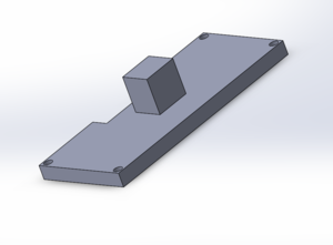
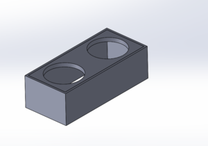
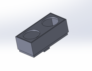
3d printed models
The dire need of fixing the sensors to the stick made us 3D print the sensor covers. So, we 3D printed the sensor covers and mounted those on the walking stick.
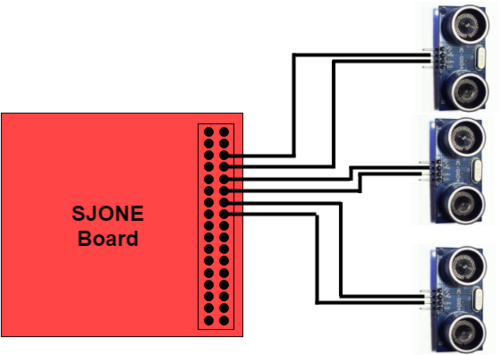
Sensor interfacing with controller
We have used Sjone board for interfacing the Ultrasonic Sensor. The ultrasonic sensors work on the concept of reflection of sound.
Sensor Pin Diagram and Interfacing with SjOne board
| Pin Name | Pin Action |
|---|---|
| P2.0 | Trigger for Left Sensor |
| P2.1 | Echo for Left Sensor |
| P2.2 | Trigger for Center Sensor |
| P2.3 | Echo for Center Sensor |
| P2.4 | Trigger for Right Sensor |
| P2.5 | Echo for Right Sensor |
Hardware Interface
Software Design
We studies the hardware interfacing of the ultrasonic sensors and now the software implementation of sensors. The basic working of the ultrasonic sensor on SJone board is just the dealing with sensors. Sending a pulse from one pin to the trigger pin enables the triggering of sensors. Then the return pulse from the echo pin is detected using the interrupt functionality on the interrupt port 2 of the SJone board. The major part of this implementation is timer. To calculate the time between the pulse send and pulse receive, timers are used. When a trigger pulse is sent to the trigger pin, the timer is started and when the reflected pulse detection is sent from the echo pin to the interrupt pin, the timer is stopped. This time difference is the time difference between the pulses. And applying the time distance equation to get the distance is the final motive.
Software Implementation and Relation of Modules
Software flow diagram
Implementation
Sensor Avoidance Algorithm
The major section of this product is the Sensor Avoidance Algorithm. If there is any obstacle from the left side, it would command the haptic driver on the left side to vibrate. If there is some obstacle on the front side, there would be vibrations on the center vibration. And similarly, if on the right side, there would be a vibration on the right side.
Algorithm
Algorithm diagram
Testing
Sensor Obstacle Avoidance
Testing & Technical Challenges
Problems in interfacing and obstacle detection Describe the challenges of your project. What advise would you give yourself or someone else if your project can be started from scratch again? Make a smooth transition to testing section and described what it took to test your project.
Include sub-sections that list out a problem and solution, such as:
Key Locator
For a blind person, keeping track of physical objects in the house can be challenging especially if they aren't found at the right place. A simple object like Key can be lost under the bed/table or maybe simply lying around a room corner. To mitigate this issue, we thought of a solution which can help a blind person to locate his/her Keys inside the house by simple press of a button. By providing the ability to search Keys using Walking Cane we can help these people save both time and effort.
Hardware Design
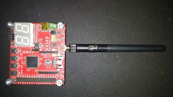
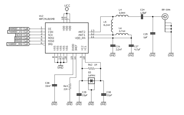
This module uses the Nordic wireless Chip Transceiver for enabling wireless communication between the Cane and Key. A in-built Nordic wireless on the SJOne board is used for board to board communication. The chip operates in the World wide ISM frequency band 2.4-2.483GHz. The radio system with nRF24L01+ has been built by simply using controller unit and few external passive components. The chip is interfaced through Serial Peripheral Interface (SPI). The boards communicate via 2.4 GHz RP-SMA Duck antennas. Below figure shows the connections of these antennas with SJOne board. Air data rate of 250 kbps, 1 Mbps and 2 Mbps is supported.
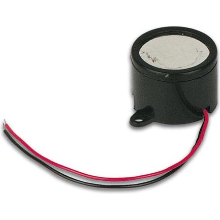
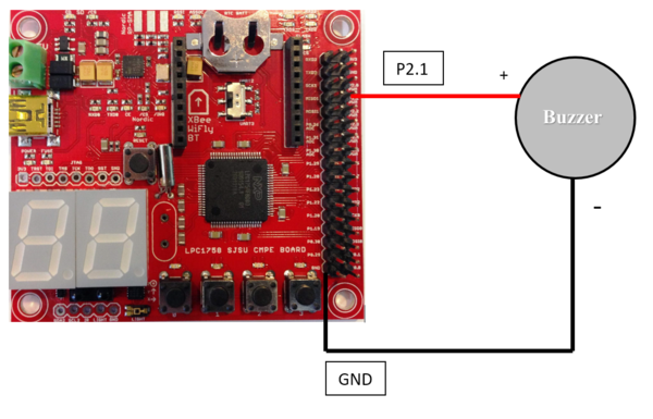
We have also made use of buzzer as part of the key. This will make a sound which can be heard within a house. The distance at which the Cane can communicate with Key generally depends on the type of antenna and the data rate. With full supply of more than 4V and 15mA, the buzzer can generate sound upto 90dB.
Hardware Interface
The hardware interface is fairly simple. A small 5V battery powers key via its on board 5V pins.The antenna is connected to the SJ One board via its SMA connector.The Nordic wireless has the following connections with the controller. SPI bus is used for communication between them.
| Nordic pins | Controller pins | Purpose |
|---|---|---|
| CE | P1.24 | Enable Tx or Rx mode |
| CSN | P0.16 | Chip Select |
| SCK | P0.15 | Clock |
| MOSI | P0.18 | Slave Data Input |
| MISO | P0.17 | Slave Data Output |
</br>
The buzzer connection with the SJOne board is as shown below. The Buzzer can work on Voltages from 3V-15V and can produce sound upto 90dB. We have used GPIO Port 2 for connecting the Buzzer.
Software Design and Implementation
1) Key Signal Transmitter : A Free-RTOS task is used to detect key press on the Cane by the blind. A mesh packet from transmitter(Cane) is sent using the following function call
Sending a packet with one data variable
mesh_form_pkt(&pkt, addr, mesh_pkt_ack, hops,1 ,&keyPressed, sizeof(keyPressed));
Packet was formed above, now send it
mesh_send_formed_pkt(&pkt);
2) Key Signal Receiver : A High Priority Free-RTOS task is used to detect signal received on the Key. On receiving the signal, a call is made to the soundBuzzer() which makes the buzzer sound.
Checking received parameter at the receiver
if(wireless_get_rx_pkt(&pkt, 100))
{
wireless_deform_pkt(&pkt,1, &iskeyPressed, sizeof(iskeyPressed));
}
The Nordic wireless API suggests that the AIR data rate, and channel number must be consistent for the wireless nodes to talk to each other. We are using two nodes in our project. Node address for the Key and Cane should be different. We are using node address as 105 for Cane and 106 for Key.The following table shows configurable parameters for setting the wireless network in sys_config.h file of the FreeRTOS for the Key. Except for the Node Address, Cane can have similar parameters.
| Parameter | Value | Remark |
|---|---|---|
| WIRELESS_NODE_ADDR | 106 | Any value from 1-254 |
| WIRELESS_CHANNEL_NUM | 2499 | 2402 - 2500 to avoid collisions among 2+ mesh networks |
| WIRELESS_AIR_DATARATE_KBPS | 2000 | Air data rate, can only be 250, 1000, or 2000 kbps |
| WIRELESS_NODE_NAME | node | Wireless node name (ping response contains this name) |
| WIRELESS_RX_QUEUE_SIZE | 3 | Number of payloads we can queue |
| WIRELESS_NODE_ADDR_FILE | naddr | Node address can be read from this file and this can override WIRELESS_NODE_ADDR |
Testing
Key Locator
Testing & Technical Challenges
Problems in interfacing jey locator Describe the challenges of your project. What advise would you give yourself or someone else if your project can be started from scratch again? Make a smooth transition to testing section and described what it took to test your project.
Include sub-sections that list out a problem and solution, such as:
GSM Module
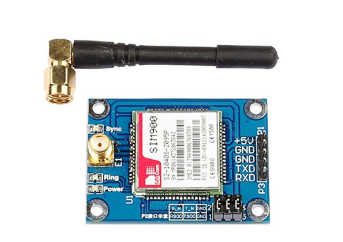
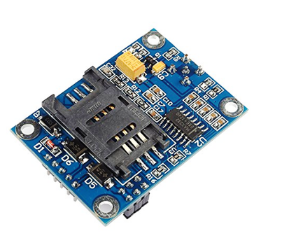
This module consist of a GSM/GPRS Sim900 modem and a press button (panic button) mounted on the stick. This GSM modem accepts a full size SIM card and can communicate using AT (Attention) commands sent from the micro controller (LPC 1758, SJone board) through UART interface at a baud rate of 115200 bits per seconds. This module requires 5 volts in order to work properly. In an emergency situation, the stick owner must press this button which will send an SMS to a registered user to take care of the blind person.
There are two led's on the modem, namely power and sync. Once the 5 volt power supply is given, the power light will turn on, and the sync led will start blinking as well. However, this sync led is very useful during testing and making sure that the SIM card has been registered on the network. If the SIM card has not been registered on the network, and/or not been inserted into the modem yet, the sync led will blink at a rate more than once every second. After the SIM card is registered the rate of blinking reduces to as low as once every three seconds.
Hardware Design
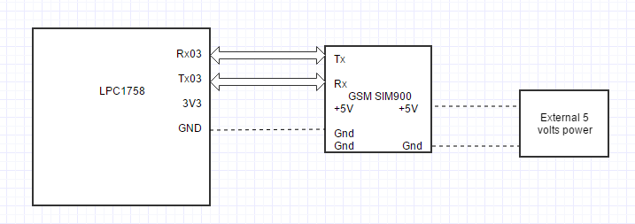
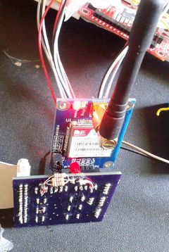
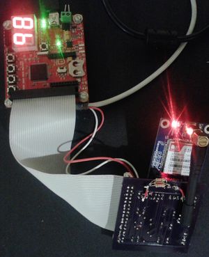
The hardware design for this module includes a GSM/GPRS Sim900 module and a switch both connecting to a common SJ one micro controller. Below is the figure of the SIM900 module from the front and the back side. Sim card is inserted at the back side of the GSM modem.
Hardware Interface
The communication protocol of GSM module with the controller is through UART which requires four wires to establish a serial communication- Rx, Tx, Ground and Vcc. Below figure shows the schematics for the connection of the GSM module with the SJ One controller.
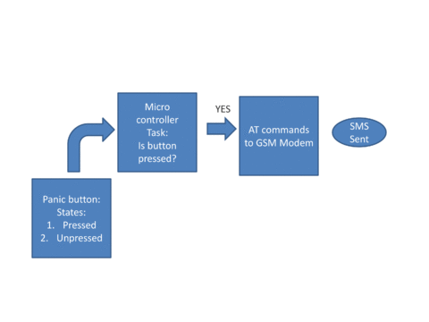
A switch used as a panic button will be used as an interrupt to the controller board's GPIO pin, which will initiate the routine to send the AT commands to the GSM module necessary for sending SMS to a cellular phone.
<Figure should appear here>
Software Design
The software design for this module will include only a panic task. This task will monitor if a stick owner has pressed the panic button or not. If the button is pressed, then the controller will send a set of AT commands required to enable GSM module to an SMS mode and be able to send a desired SMS to the cellular phone. Below figure shows the control flow of GSM module.
The essence of writing code for the GSM module is the proper usage of AT commands provided by the GSM manufacturer. GSM modem understands the AT commands, which are used as a prefix with every command send to it and followed by a carriage return (\r character from the controller). The SIM900 modem implements the combination of GSM07.05, GSM07.07, V.25ter, and the AT commands developed by SIMCom. Syntactically, AT commands can be split into three categories, but the most used ones, that are also used for this project are: basic and extended.
Basic AT commands: These are the commands which are used to do basic operations such as Dial (ATD), Answer (ATA), Hang up (ATH), etc which are also used for dial-up modems.
Extended AT commands: Besides the basic commands set there are commands which are specific to the GSM technology. These commands can be used to read, write, delete, and send the SMS. These commands can operate in different modes such as test, read, write, and execution mode. All the extended commands starts with AT and ends with carriage return.
Configure the GSM module for sending SMS:
a) Sending to a single subscriber (one message)
1. AT<Carriage Return>. A response of OK means that connection between controller and modem is working fine.
2. AT+CMGF=1. This tells the modem that the text mode for the SMS should be used, where as the other mode, PDU, can be set by setting the value to 0.
3. AT+ CMGS= "1530*****61" <Carriage Return> =>message <ctrl-z>. This is the format for sending an SMS by using +CMGS command.
b) Sending to multiple subscribers
It will be a choice for a stick-owner to choose if he has to send an emergency message to a single person, or there is more than one person to whom he wants to issue the message. In case of multiple senders, sending using +CMGS is not as efficient, as it may take upto a min. from the time blind person presses the panic button to the time it reaches to his 4th friend. In case of issuing the same message to multiple cell phones, sending a message from storage is more efficient.
Below is the sequence of the AT commands from sending from SIM storage.
1. AT
2. AT+CMGF=1. For SMS mode
3. AT+CPMS="SM","SM". Format for +CPMS is +CPMS=storage1[,storage2[storage3]]. Messages are read and deleted from storage1. Messages are written to storage2. Storage3 defines the memory location to store the received messages. However, if we are not concerned with receiving text, we can ignore this optional parameter.
4. AT+CSCA="+12063130004”. This AT command is to set the SMSC address to where the messages are sent first and dispatched for the destination number. For T-mobile network this number is +12063130004. This # can be found from the cell phone in the message settings.
5. AT+CMGW="1530*****61",129,"STO UNSENT" <Carriage Return> Message <ctrl-z>. This AT command writes the messages to the memory space provided in the above +CPMS command. Second and third parameters are optional. First parameter is the destination number which is stored along with the message as well. Important point to note is that the message required to be written to the SIM only once. Once the message has been written to the particular index, this write function may not be required to call.
6. AT+CMSS=1,"1530*****61". +CMSS is used to send a message from the storage. First parameter of +CMSS is the index of the memory location from where to send the message. Second parameter is to where to send the message.
Other useful AT commands that were used during the testing as well as for the final code sequence of the AT instructions:
1. AT+CSCS = "GSM". SIM900 defaults to IRA character set. This AT command change it to GSM character set.
2. AT+CMEE = 2. This command is used to get the indication of an error related to the ME functionality. Parameter 2 enables the +CME error in verbose form. For example, +CME error: sim is not inserted. However, 0 parameter value is default and used to disable +CME error, only 'error' is displayed in case of some error.
3. AT+CREG=2;AT+CREG=?. This command is used to tell whether the SIM card is registerd on the network. parameter 2 we get the registration result with the location information.
4. AT+CMGR=1;AT+CMGD=1,4. +CMGR is used to read the messages from the memory storage. Whereas, +CMGD is used to delete messages from the storage. First parameter is the index of the memory location in both instructions, however parameter 4 in +CMGD implies to delete all the messages. Other parameters (0-4) can be used as per requirement.
5. AT + CPIN?. This command may come handy when for example your sim requires a password. For us, we got the response READY, indicating that SIM is good to use, and has no kind of passwords, such as SIM PIN or SIM PUK.
6. AT+CMGD=?. This command responds about the list of supported indexes and the list of supported flags, then OK. For example, I would get the response as +CMGD: (1-30),(0-4), which means that I can assign any index value from 1 to 30 for my SIM memory to store messages, and it supports all five flag values defined in the Sim specification.
Implementation
Before getting started writing the AT (Attention) commands for the GSM modem, it would be recommended to check whether the module is functioning correctly by following the three simple steps:
First, check if both the power light and the sync light are glowing. While the power light should glow steady, the sync light will blink more than once every second.
Second, insert a SIM into the slot, give a call to the GSM module inserted SIM, if the call passes through, it means the SIM has been registered on the network and can be used with the module and the GSM module is working fine as well.
Third, check for the blinking ‘sync’ light on the GSM module. Initially, this light blinks at a faster rate, but once the SIM has been registered over the network, frequency of blinking reduces to as low as once in every three seconds.
Next step includes doing some research about your SIM card and your GSM modem neglecting which may otherwise interfere with the working of a GSM modem:
One, Figure out the cellular phone’s GSM frequency coverage and whether the GSM modem works for this frequency band. For instance, Metro PCS and T-mobile, both provide a wireless phone service that operates at 1900 MHZ frequency band.
Two, Knowledge about your SIM card and service provider. I have a MetroPCS SIM, after consulting with the customer service regarding using the unregistered device (GSM module) on their network they reciprocated in negative; however, they suggested that in order to register a GSM modem, I needed to supply them with the IEMI # of my modem. And, to use my cell again I had to provide back the IEMI # of my cell phone. As it sounds a tedious task, other solution was to check other SIM card from different network provider, and it turned out that the T mobile SIM card works without going through the process explained above.
Three, Make sure SIM-card does not have a SIM lock activated.
After making sure that the above steps have been successfully checked, writing code for the GSM modem was started. Below is the code snippet for making a phone call, which requires a minimum of AT commands:
      void give_a_call(void)
       {
           const char at_init[] = { "AT\r" };
           const char phone_mode[] = { "AT+CMGF=0\r" };
           const char call_num[] = {"ATD1530*****61;\r\n"};
           const char ctr_z = 0x1A;
           char response[30];
           Uart3 &msz = Uart3::getInstance(); //initializing UART3 for communication
           msz.init(115200, 512, 512);
           delay_ms(2000); //wait for 2 sec. before GSM is ready to accept AT commands on startup
           msz.putline(at_init); //second param of put/putChar is optional, defaults to portMAX_DELAY
           delay_ms(2000);
           msz.putline(phone_mode);
           delay_ms(150);
           msz.putline(call_num);
           delay_ms(5000); //wait for some time while you're making a phone call
           msz.gets(response, 30);
           printf("%s\n",response);
         }
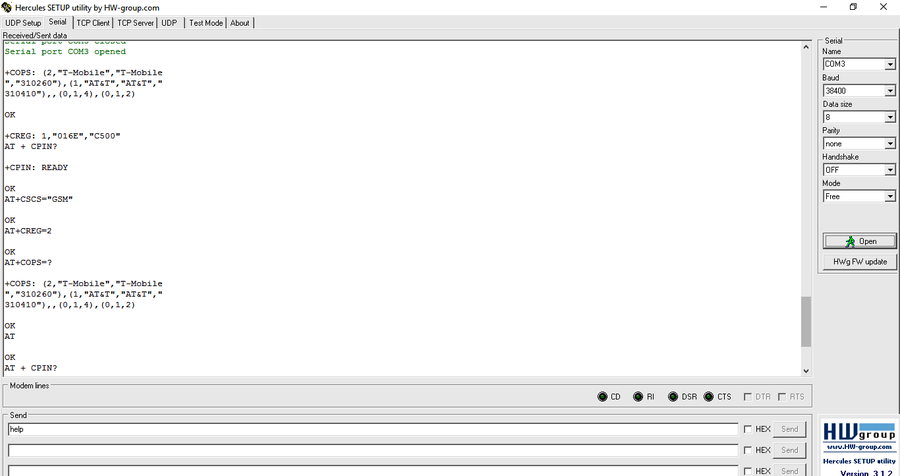
As shown in the above code, at the end, the response has been captured and outputted on the screen. The response of each AT command can be outputted if the task is in forever loop by storing the response from the GSM modem in an array (datatype char), i.e char response[30], such as msz.gets(response, 30) shown in above code snippent and then using the printf to see the response at the Hercules.
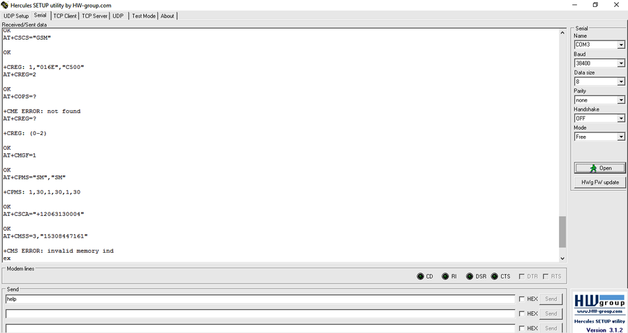
Figure a, shows the response at the terminal when the GSM is successfully sending the SMSs. Whereas, figure b, shows the response at the terminal when AT command tries to send an SMS from the memory location where an SMS has not been already written.
The explanation for the terminal output for figure b. is that the AT command +CMSS tries to send an SMS from the SIM memory with index 3. However, the AT command above CMSS, +CPMS responds that only the memory index '1' has been written with an SMS. That is the reason, we get the +CMS error: invalid memory index. To get rid of the error, either there should more SMS be written so that the index 3 actually has the intended SMS, or change the index from 3 to 1 in the AT command +CMSS, that is, AT + CMSS= 1, 1530*****61.
Testing
GSM module
Initially, the GSM module was tested with jumper wires connecting directly to the micro controller (LPC 1768); meanwhile, the PCB design for integration of all the sensors as well as for LPC controller connection and GSM connection was ready. Then, testing was done with PCB board.
Testing & Technical Challenges
Problems in interfacing and obstacle detection Describe the challenges of your project. What advise would you give yourself or someone else if your project can be started from scratch again? Make a smooth transition to testing section and described what it took to test your project.
Include sub-sections that list out a problem and solution, such as:
Haptic Feedback
A blind person can not see things. He can only feel the sense of “touch”. In order to assist him to detect obstacles, a novel technique called haptic feedback is used in our project. Whenever an obstacle is detected by the sensors, motors fixed on the smart stick will vibrate with different effects. Based on the pattern and amplitude of vibration, he can realise about an upcoming obstacle in that direction and can thus move in the other appropriate direction. The vibration patterns vary depending on the direction and proximity of the obstacle. This module consist of a haptic vibrator and motors.
Hardware Design
The hardware design for haptic feedback consists of haptic driver DRV2605L and Precision Haptic 10 mm Linear Resonant Actuator. The low voltage and flexible haptic driver is used to control LRA (Linear Resonant Actuator) and ERM (Eccentric Rotating Mass) type of motors. This driver removes the difficulty of altering the PWM signal by providing a huge haptic library that can produce 127 different vibration patterns on the motors. The IN/TRIG pin provides external trigger control of the GO bit that launches the desired waveforms. The LRA based motor has excellent haptic characteristics and can vibrate with various amplitude, frequency and effects based on the input.
Hardware Interface
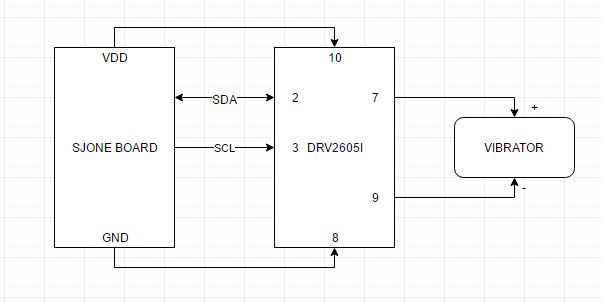
The haptic driver DRV2605L is interfaced to SJONE board using I2C protocol through 3 wires namely Serial clock (SCL), serial data lines (SDA) and common ground. The vibration DC motor is connected to haptic driver through its differential output lines.
Below table lists the pin connection between SJONE board and haptic driver
| Sl. No | Pin on SJONE board | Pin on Haptic driver | Purpose |
|---|---|---|---|
| 1 | SDA | 2(SDA) | Data line |
| 2 | SCL | 3(SCL) | Clock Line |
| 3 | GND | 8(GND) | Common Ground |
| 4 | VCC | 10(VCC) | Power Supply |
Below tables shows the pin connection between haptic driver and vibration motor
| Sl. No | Pin on Haptic driver | Pin on Vibration motor | Purpose |
|---|---|---|---|
| 1 | 7 | POSITIVE LINE | Positive differential output |
| 2 | 9 | NEGATIVE LINE | Negative differential output |
Software Design
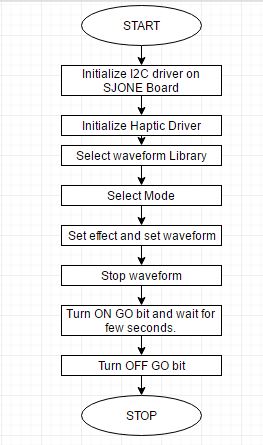
A task is created to implement the functionality of haptic feedback. Initialization of certain modules such as haptic driver and i2c slave has to be carried out before the actual functionality could be implemented. After this step, selection of library and setting of appropriate mode is done. Once these steps are carried out, the motors are ready to vibrate with any pattern based on the Effect value. A desired value is set in the waveform function and GO bit is turned ON. This would play the desired waveform until the GO bit is turned OFF. Whenever an obstacle is detected in the left direction, the motor would vibrate with a single click frequency, double click for obstacle in right direction and triple click for front direction. Based on the frequency pattern, a blind person can understand the direction in which the obstacle is present and can then move in the appropriate direction. Also if the distance between the obstacle and the user is more, it will vibrate with a soft buzz and if the distance is less, it will vibrate with a loud buzz. Based on the buzz amplitude, user can know the proximity of the obstacle.
Implementation
In order to interface the haptic driver to SJONE board, additional slave device has to be configured in the I2C protocol by setting appropriate values in the I2C registers namely I2ADR, I2MASK and I2CONSET. The slave address is found to be OXB4 upon using i2c discover command. Once the slave device has been properly configured, i2c transactions such as read and write to registers in haptic driver can be performed. In order to communicate with the haptic driver, certain initialization has to be done which mostly involves configuring the registers.
Some of these steps include:
1. Wake up the driver out of standby mode by setting “0”. 2. Switch off real time playback by setting “0”. 3. Enable strong click feature by setting value “1”. 4. Disable overdrive by setting value “0”. 5. Set “0” values to sustain positive and negative registers.
The below code shows haptic driver initialization sequence
bool haptic_driver_init()
{
     hapdrivevalue=0x00;
     i2cobj.writeReg(slaveAddr,DRV2605_REG_MODE,hapdrivevalue);
     i2cobj.writeReg(slaveAddr,DRV2605_REG_RTPIN,hapdrivevalue);
     hapdrivevalue=0x01;
     i2cobj.writeReg(slaveAddr,DRV2605_REG_WAVESEQ1,hapdrivevalue);
     hapdrivevalue=0x00;
     i2cobj.writeReg(slaveAddr,DRV2605_REG_WAVESEQ2,hapdrivevalue);
     i2cobj.writeReg(slaveAddr,DRV2605_REG_OVERDRIVE,hapdrivevalue);
     i2cobj.writeReg(slaveAddr,DRV2605_REG_SUSTAINPOS,hapdrivevalue);
     i2cobj.writeReg(slaveAddr,DRV2605_REG_SUSTAINNEG,hapdrivevalue);
     i2cobj.writeReg(slaveAddr,DRV2605_REG_BREAK,hapdrivevalue);
     hapdrivevalue=0x64;
     i2cobj.writeReg(slaveAddr,DRV2605_REG_AUDIOMAX,hapdrivevalue);
     hapreadvalue = i2cobj.readReg(slaveAddr,DRV2605_REG_FEEDBACK);
     hapdrivevalue = hapreadvalue & 0x7f;
     i2cobj.writeReg(slaveAddr,DRV2605_REG_FEEDBACK,hapdrivevalue);
     hapreadvalue = i2cobj.readReg(slaveAddr,DRV2605_REG_CONTROL3);
     hapdrivevalue = hapreadvalue | 0x20;
     i2cobj.writeReg(slaveAddr,DRV2605_REG_CONTROL3,hapdrivevalue);
     return true;
}
After the configuration of the registers is done, library is selected for choosing a waveform and mode is set to initiate trigger. Now a proper value for “effect” is chosen to get a particular vibration pattern and is set to the waveform function register slot. Upon writing a value “1” to the GO bit, waveform is launched and user can sense the haptic feedback. Setting value “0” to GO bit cancels the waveform and thereby switching off feedback.
The below code shows the configuration of certain registers for selecting library, setting waveform etc.
bool hapWrite(uint8_t slot, uint8_t value, hapticfunction hvalue) {
   switch(hvalue)
   {
       case SETWAVEFORM:
           hapdrivevalue = value;
           i2cobj.writeReg(slaveAddr,DRV2605_REG_WAVESEQ1+slot,hapdrivevalue);
        break;
        case SELECTLIBRARY:
            hapdrivevalue = value;
            i2cobj.writeReg(slaveAddr, DRV2605_REG_LIBRARY, hapdrivevalue);
        break;
        case GO:
             hapdrivevalue = value;
             i2cobj.writeReg(slaveAddr,DRV2605_REG_GO,hapdrivevalue);
             break;
         case SETMODE:
             hapdrivevalue = value;
             i2cobj.writeReg(slaveAddr,DRV2605_REG_MODE,hapdrivevalue);
             break;
         case SETREALTIMEVALUE:
             hapdrivevalue = value;
             i2cobj.writeReg(slaveAddr,DRV2605_REG_RTPIN,hapdrivevalue);
             break;
         }
Below are some of the Registers used to while initializing the DRV2605L module.
- DRV2605_REG_STATUS 0x00
- DRV2605_REG_MODE 0x01
- DRV2605_MODE_INTTRIG 0x00
- DRV2605_MODE_EXTTRIGEDGE 0x01
- DRV2605_MODE_EXTTRIGLVL 0x02
- DRV2605_MODE_PWMANALOG 0x03
- DRV2605_MODE_AUDIOVIBE 0x04
- DRV2605_MODE_REALTIME 0x05
- DRV2605_MODE_DIAGNOS 0x06
- DRV2605_MODE_AUTOCAL 0x07
- DRV2605_REG_RTPIN 0x02
- DRV2605_REG_LIBRARY 0x03
Testing: Haptic Feedback
We tested this module by giving different values to the the waveform register and observed the following patterns.
| Sl. No | Effect number | Pattern |
|---|---|---|
| 1 | 1 | SINGLE CLICK 100% |
| 2 | 10 | DOUBLE CLICK 100% |
| 3 | 12 | TRIPLE CLICK 100% |
| 4 | 14 | STRONG BUZZ 100% |
Testing & Technical Challenges
Describe the challenges of your project. What advise would you give yourself or someone else if your project can be started from scratch again? Make a smooth transition to testing section and described what it took to test your project.
Include sub-sections that list out a problem and solution, such as:
My Issue: GSM Module
1. 5 volt supply is necessary for the proper working of the GSM SIM900 modem. If the 3.3 V supply from the SJOne is used, the sync light will not glow; other observation in this context was either too fast blinking (4-5 times a second) or not blinking at all are the indications that the power to GSM modem is not correct which as per datasheet should be 5 V with around 2 A current (over 1 A). That is why a dedicated 5 volt battery was required. During testing 5 V output from the laptop was plugged out through the USB port.
2. It is important to adjust the delay between the AT commands. Since the delay between each AT command is necessary, and one AT command should wait till the previous AT command has responded back. Initially, the delay between the AT command for sending an SMS from storage was kept at 100 ms, and the SMS was not sent. Solution was to gradually increasing the delay. It was figured out that the delay of 200ms was optimal for the proper execution of these two particular AT commands.
Conclusion
Conclude your project here. You can recap your testing and problems. You should address the "so what" part here to indicate what you ultimately learnt from this project. How has this project increased your knowledge?
Project Video
Upload a video of your project and post the link here.
Project Source Code
References
Acknowledgement
Any acknowledgement that you may wish to provide can be included here.
References Used
Nordic Wireless [1]
Haptic Driver [2]
Haptic Vibrator [3]
Appendix
You can list the references you used.
