S16: Expendables
Contents
Grading Criteria
- How well is Software & Hardware Design described?
- How well can this report be used to reproduce this project?
- Code Quality
- Overall Report Quality:
- Software Block Diagrams
- Hardware Block Diagrams
- Schematic Quality
- Quality of technical challenges and solutions adopted.
Project Title
Abstract
This section should be a couple lines to describe what your project does.
Objectives & Introduction
Show list of your objectives. This section includes the high level details of your project. You can write about the various sensors or peripherals you used to get your project completed.
Team Members & Responsibilities
Schedule
| Sl. No | Start Date | End Date | Task | Status | Actual Completion Date |
|---|---|---|---|---|---|
| 1 | 3/07/2016 | 3/13/2016 | Components buying | Completed | 3/18/2016 |
| 2 | 3/14/2016 | 3/20/2016 | LED panels study | Ongoing | |
| 3 | 3/28/2016 | 4/03/2016 | Raspberry Pi 3 study | ||
| 4 | 4/04/2016 | 4/10/2016 | Pixel Driver Design | ||
| 5 | 4/11/2016 | 4/17/2016 | PCB Design | Completed | 3/30/2016 |
| 6 | 4/18/2016 | 4/24/2016 | Testing Text Display | ||
| 7 | 5/25/2016 | 5/01/2016 | UI Webserver | ||
| 8 | 5/02/2016 | 5/08/2016 | Final Testing and Debugging |
Parts List & Cost
Give a simple list of the cost of your project broken down by components. Do not write long stories here.
Design & Implementation
Hardware Design
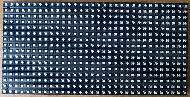
LED Panels
The display panels use multiplexing to draw picture information, which means that the rows and columns are updated fast than the human eye can process. If the updating speed is fast enough, eyes will see a complete picture without flickering. The updating process is as follows
- Select the row to be updated.
- Output the desired column data on selected row.
Row Selection
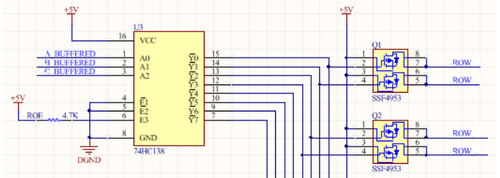
Row selection is done by using a 3-to-8 address decoder (74HC138D). There are three address inputs to the display marked A, B and C. Based on the truth table, only one input is active (low) at a time.
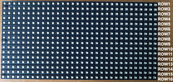
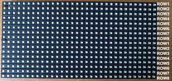
Since the panels has 16 rows, the 3-to-8 address decoder select rows in parallel. For example, when the 1st row (Row1) is selected, it also selects the 9th row (Row9). Using this technique implies that we must supply data for the columns for two unique rows at a time.
The outputs of the decoder is connected to a P-Channel MOSFET, because the decoder itself can only handle low currents and cannot drive a row of LEDs directly. The P-Channel MOSFET provides the high current needed to drive a row of LEDs.
The decoder outputs are shared between every 8 outputs (1 and 9, 2 and 10, repeating that pattern until row 8 and 16).
Column Selection
The column data is stored in a 16-bit serial-in, parallel-out shift register. Since the display is 32 pixels wide, two shift registers must be chained together. The shift register is designed to work with LEDs and implements a constant-current system that ensures the LED brightness remains uniform. The panels that we are using utilize SCT2026 shift registers. These are 16-bit Serial-In/Parallel-Out registers.
There are 12 of these shift registers on the display. 3 each are used to hold the Red, Green, and Blue data for 1 of 4 quadrants of the display. (3 colors * 4 quadrants = 12 chips)
For drawing 16 rows using the 8 outputs of the decoder, we must have unique data for each row pair. When Row 1 and Row 9 are selected, we must provide each row with unique data. This forces us to use two different shift registers for each row pair, an upper register and a lower register. Because of this, the display is divided into an upper half and a lower half. The data is shifted into the top half via the R1, G1 and B1 signals on the connector. The bottom half’s data is supplied by the R2, G2 and B2 signals on the connector. Then, since our display is 32 pixels wide, we must use 2 shift registers to hold all 32 bits of pixel data for a single row. This creates the left and right halves of the display. Each quadrant of the display is controlled by 3 shift registers, one for each color. First, Row 1 and Row 9 are selected. 32 bits of data are shifted into each color’s shift register (R1, G1, B1), and then latched. At the same time, 32 bits of data are also shifted into each color’s shift register for the bottom half (R2, G2, B2), and then latched. The process repeats 7 more times, each time incrementing which rows are selected, until every line has been updated.
Hardware Interface
In this section, you can describe how your hardware communicates, such as which BUSes used. You can discuss your driver implementation here, such that the Software Design section is isolated to talk about high level workings rather than inner working of your project.
PCB Design
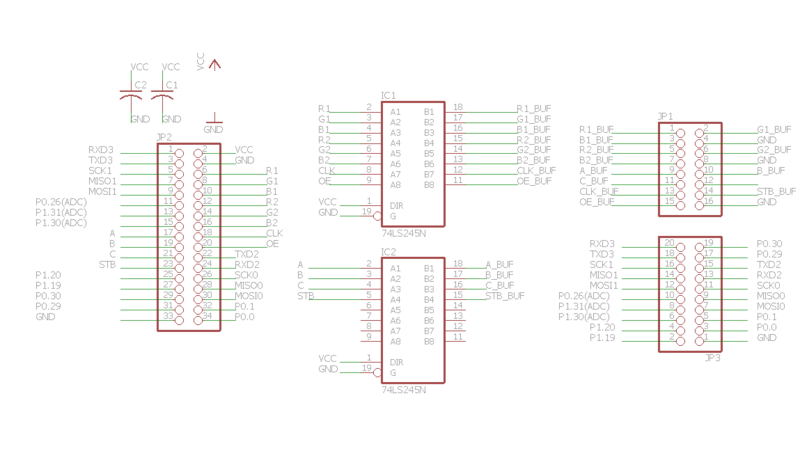
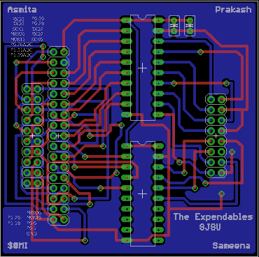
The LED panels use 74HC245 line drivers, these transceivers require 5v logic levels whereas the SJONE board only supports 3.3v logic. In order to drive the LED panels from 3.3v GPIO pins of the SJONE board, level-shifting IC is used to level shift signals from 3.3V to 5V and shield the SJONE board GPIOs from overloading. For this purpose, a PCB was designed in EAGLE. The PCB attaches to GPIO pins of SJONE board and provides easily accessible, level-shifted output for the LED panels. The PCB also breaks-out free pins so that they can be used for other purposes.
Software Design
Show your software design. For example, if you are designing an MP3 Player, show the tasks that you are using, and what they are doing at a high level. Do not show the details of the code. For example, do not show exact code, but you may show psuedocode and fragments of code. Keep in mind that you are showing DESIGN of your software, not the inner workings of it.
Implementation
This section includes implementation, but again, not the details, just the high level. For example, you can list the steps it takes to communicate over a sensor, or the steps needed to write a page of memory onto SPI Flash. You can include sub-sections for each of your component implementation.
Testing & Technical Challenges
Describe the challenges of your project. What advise would you give yourself or someone else if your project can be started from scratch again? Make a smooth transition to testing section and described what it took to test your project.
Include sub-sections that list out a problem and solution, such as:
My Issue #1
Discuss the issue and resolution.
Conclusion
Conclude your project here. You can recap your testing and problems. You should address the "so what" part here to indicate what you ultimately learnt from this project. How has this project increased your knowledge?
Project Video
Upload a video of your project and post the link here.
Project Source Code
References
Acknowledgement
Any acknowledgement that you may wish to provide can be included here.
References Used
List any references used in project.
Appendix
You can list the references you used.
