F18: Zero Zero UFO
Contents
Grading Criteria
- How well is Software & Hardware Design described?
- How well can this report be used to reproduce this project?
- Code Quality
- Overall Report Quality:
- Software Block Diagrams
- Hardware Block Diagrams
- Schematic Quality
- Quality of technical challenges and solutions adopted.
Project Title
Zero Zero UFO
Abstract
Bringing a classic game back to life using Embedded Processors and FreeRTOS will help bring a new take to the basic handheld game. We decided to develop the UFO survival game. The objective is to keep the UFO flying for as long as you can whilst avoiding randomly generated obstacles and the other players ufo. The players will control their respective UFOs with the help of the "Accelerometer" sensor present on the SJone board. The ufo can move in either of these directions; Upward, Downward, Forward, Backward , to avoid crashing. The obstacles will move from Right to Left but the Players' UFOs will stay in the field of vision, i.e. they will always be on the screen. The obstacles will have random spacing and random size, testing the users focus. Player who survives longer wins the Game.
Objectives & Introduction
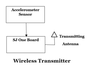
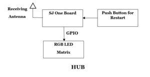
Primary objective of this project was to write efficient code to develop a game using FreeRTOS. SJOne Boards act as the heart of the project with one acting as the hub and one acting as the wireless controller. The accelerometer sensor on the SJOne board which is connected via I2C is used to register the controller orientation. This orientation is then transferred to the hub using a wireless packet. Once the hub, receives the orientation in the queue, game logic decides wether to move the UFO up or down. The obstacles are generated randomly and are moved from right to left on the LED matrix. If player's UFO collides with any of the obstacles its game over. The speed of obstacle movement increases as the levels goes up.
Game development is a big industry and this project helps us in understanding logic development and manipulating FreeRTOS features to get a good and interesting output. The project includes following modules:
- 1. Wireless Controller: 1 SJOne board is used as the controller. It wirelessly transmits orientation.
- 2. Master Hub: The other SJOne Board is used as the master device. The game logic resides on this board. It is also used to drive the display.
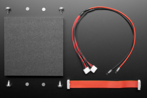
- 3. Display Module: Adafruit 64x64 Led Matrix display is used to display the game. This is driven by the GPIO pins on the master SJOne Board.
The Game
- Wireless UFO game.
- Press switch on controller to start the game.
- Randomly generated obstacles of varying sizes.
- Tilt controller up or down to fly the UFO.
Team Members & Responsibilities
- Neel Patel
- LCD Interfacing
- UFO algorithm
- Start Screen
- Report
- Aman Chandan
- Wireless Communications
- Accelerometer value filtering
- Oliver Zhu
- Wireless Communication
- Himanshu Gunjal
- LCD Interfacing
- Start Screen
- Random Obstacle Algorithm
- Pooja Baviskar
- PCB Design
- Report
Schedule
| Week# | Date | Task | Activities | Status | Completion Date |
|---|---|---|---|---|---|
| 1 | 10/16/18 |
|
|
|
|
| 2 | 10/23/18 |
|
|
|
|
| 3 | 10/30/18 |
|
|
|
|
| 4 | 11/6/18 |
|
|
|
|
| 5 | 11/13/18 |
|
|
|
|
| 6 | 11/20/18 |
|
|
|
|
| 7 | 11/27/18 |
|
|
|
|
| 8 | 12/4/18 |
|
|
|
|
| 9 | 12/8/18 |
|
|
|
|
Parts List & Cost
| Sr No# | Part | Source | Price |
|---|---|---|---|
| 1 | SJOne Board | Preet | $80 |
| 2 | 64x64 LED Matrix | Adafruit | $74.95 |
| 3 | PCB | JLC PCB | $20 |
| 4 | Power Jack | Excess Solutions | $6.99 |
Design & Implementation
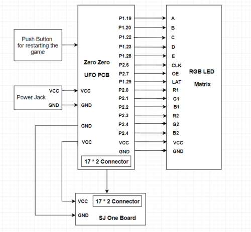
This section talks about how the various modules of the project were designed and implemented. The system block diagram is given below. The hardware utilizes 2 SJOne boards and a 64x64 Adafruit LED matrix display.
1. Wireless Module
In this section, you can describe how your hardware communicates, such as which BUSes used. You can discuss your driver implementation here, such that the Software Design section is isolated to talk about high level workings rather than inner working of your project.
2. Master Module
Show your software design. For example, if you are designing an MP3 Player, show the tasks that you are using, and what they are doing at a high level. Do not show the details of the code. For example, do not show exact code, but you may show psuedocode and fragments of code. Keep in mind that you are showing DESIGN of your software, not the inner workings of it.
3.Display Module
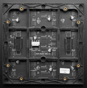
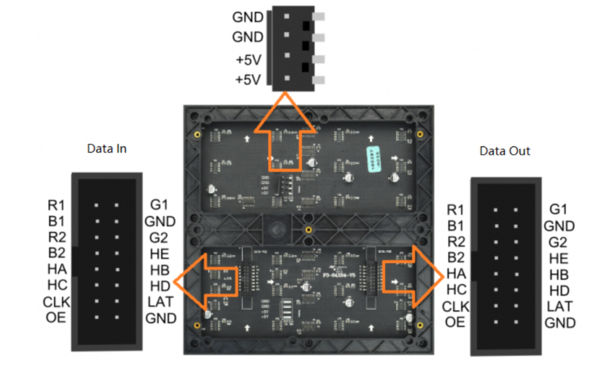
This is a 64x64 RGB LED Matrix Panel, it has 4096 full-color RGB LEDs in all. Each LED can be independently addressed and controlled. It requires at least 13 digital GPIOs to control the LED matrix. The led matrix has 2 IDC connectors (DATA_IN, DATA_OUT) on the back, you can cascade multiple panels and make a huge screen together. There are two 5*32 decoders used for decoding the address rows. Two 3*64 bit shift registers are used for selecting the colors. This is done by clocking the 64 bit shift registers. There are 5 address lines A,B,C,D,E,F for selecting the rows and six 64 bit registers each for R1,G1,B1,R2,G2,B2 for illuminating the leds. A single clock is interfaced to all these 6 64bit shift registers.Once the clocking and shifting the register is completed we need to latch this data to the register. The register data is sent out to all the row lines and that Row line which is pulled low by the decoder will receive this data and corresponding pixels are turned on.
Board Overview
Pin Description
| Label | Name | Function |
|---|---|---|
| 1 | DR1 | High R data |
| 2 | DG1 | High G data |
| 3 | DB1 | High B data |
| 4 | DR2 | Low R data |
| 5 | DG2 | Low G data |
| 6 | DB2 | Low B data |
| 7 | A | A line selection |
| 8 | B | B line selection |
| 9 | C | C line selection |
| 10 | D | D line selection |
| 11 | E | E line selection |
| 12 | F | F line selection |
| 13 | CLK | CLOCK |
| 14 | LAT | LATCH |
| 15 | OE | Output Enable |
| 16 | GND | GND |
Specification
- Operating voltage: DC 5V
- Average power consumption: <500W/㎡
- Maxim Power Consumption: <1000w/㎡
- Pixel: 64x64=4096
- Level of viewing Angle: ≧160°
- Control mode: Synchronous control
- Drive mode: 1/16 scan rate
- Repetition frequency: ≧60Hz
- White Balance Brightness: ≧1200cd/㎡
- Refresh frequency : ≧300Hz
- MTTF: ≧5000 hours
- Service Life: 75000~100000 hours
- Pixel pitch: 3mm
- Dimension: 190 * 190 * 14.5 mm / 7.48 * 7.48 * 0.57 inches
- Thickness: 11mm
Row Selection
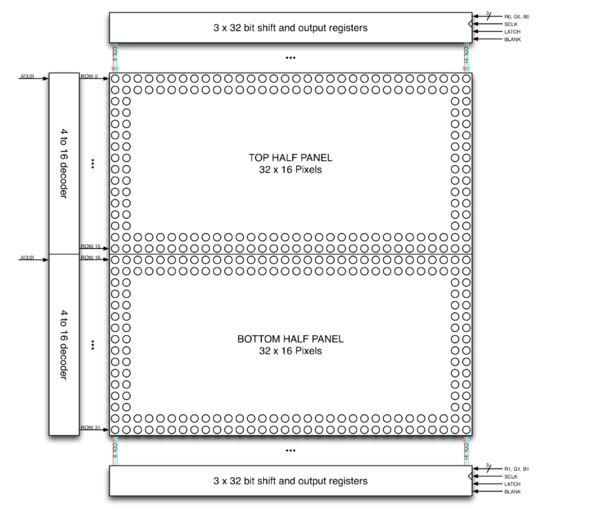
The rows are driven using four address bits and an address decoder. The four-bit address input to the row drivers is decoded and the two row drivers corresponding to that address will be turned on. When A[3:0] is 0, rows 0 and 16 of the display are turned on. When A[3:0] is 1, rows 1 and 17 of the display are turned on. This pattern continues until A[3:0] is 15 and rows 15 and 31 are turned on.
In addition to the row and column logic and drivers, the display has a blanking input. This input is most likely connected to the column drivers. When the blanking signal is asserted, all of the pixels are turned off and the display will be black. When the blanking signal is deasserted, the addressed rows and columns will be driven and the corresponding pixels illuminated. To display an image without flickering and ghosting, all of these signals must be used and properly sequenced when driving the panel.
Column Selection
The panel contains six sets of column drivers; three for the top half of the display and three for the bottom. Each driver has 32 outputs. The three drivers for the top of the display drive the red, green, and blue chips in each of the 32 columns of LEDs in rows 0 to 15 of the panel. The three drivers for the bottom of the display drive the red, green, and blue chips in each of the 32 columns of LEDs in rows 16 to 31 of the panel.
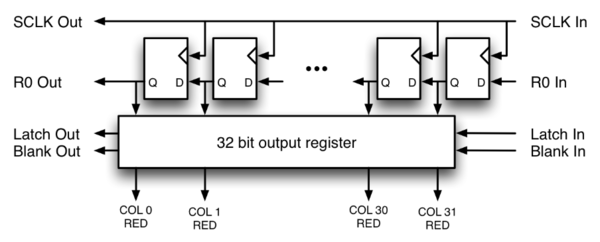
Each of the drivers has a serial data input, a blanking input, a shift register, and a parallel output register as shown below in Figure 3. The data present on the serial data input is shifted into the shift register using the SCLK signal. After an entire row of data has been shifted in to the shift register, the LATCH signal is used to transfer the row of pixel data from the shift register into the parallel output register. If a bit in the output register is a ‘1’ and the blanking input is deasserted, the driver for that column will be enabled; otherwise, the driver will be turned off. Data is shifted from the right edge of the display to the left edge of the display. In other words, the first bit shifted in will be displayed on the left edge of the display and the last bit shifted in will be displayed on the right.
The red, green, and blue column drivers for the top half of the display are attached respectively to the R0, G0, and B0 data inputs. The red, green, and blue column drivers for the bottom half of the display are attached respectively to the R1, G1, and B1 data inputs. All six of the 32-bit drivers share common SCLK, LATCH signals.
Pin Configuration
The diagram shows the pin connection between SJ One board and LED Matrix. The five address lines used for selecting the rows, R1, G1, B1, R2, B2, G2 used for illuminating the LEDs, CLK for shift register and LAT are connected to the 14 GPIO pins. The power is given to the board and LED matrix using a 5 volt 5 amperes power adapter. This is split between the SJ One board and the LED Matrix. There is also a push button which is used for restarting the game.
PCB
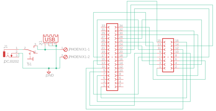
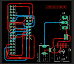
After testing all the components individually on breadboard, we soon realized that we would need to create a custom PCB in order to minimize the wired connections. We used Eagle 9.2.2 software to design a 2 layer PCB. We have designed a circuit which supplies 5V power to SJ One board and LED Matrix through a switch using phoenix connector and female USB connector. There is also one 17*2 female connector which is connected to the HUB 75E connector that is used to transfer data to the LED Matrix.
EAGLE Connector List
| Sr.No | Components |
|---|---|
| 1 | DC Jack |
| 2 | Female USB Connector |
| 3 | SPST Switch |
| 4 | Phoenix Connector |
| 5 | 17*2 Female Connector |
| 6 | HUB 75E Connector |
After the schematic is ready we generate the board file. The width for the PCB tracks is 40 mil which can carry 5 Amperes of current and the size of our PCB is 61 mm*51 mm. The PCB board layout is shown in the figure below:
<Bug/issue name>
We had a few issues with the hardware and few bugs in the software while developing the game. They are listed in the section along with the solution we found to fix them.
- 1. Display Lines Mismatch: This was a problem with the Adafruit LED matrix we had bought for this project. The LINE 32 took LINE 0 place. This resulted in LINE 0 to LINE 31 getting incremented by one. That is, LINE 1 became LINE 0, LINE 2 became LINE 1 and so on. We fixed this problem by modifying the graphics library and we decremented the value of "y". So , when y is between 1-32 we decrement it by 1 and when y=0 we make it y=31. this maps y=0 to LINE 0. Similarly, when y was between 32-63 we decremented it by 1 and when y=32 we make it y=63. This maps LINE 63 with y=63.
- 2. Wireless Communication Problem: Our wireless communication was not working properly. The "orientation" of the controller was being transmitted properly but the receiver was not receiving the data correctly. The issue was that the wireless task had been disabled on the receiver side, so, even though the controller was transmitting the orientation the receiver was having problem in registering it from the nordic level and put it into the queue from which it could be read. The interesting to notice here was even with the wireless task disabled we were receiving 1 or 2 initial values, albeit not timely. This problem was solved by enabling the wireless task and using channel 2510(FCC restricted channel) to avoid interference.
Conclusion
Conclude your project here. You can recap your testing and problems. You should address the "so what" part here to indicate what you ultimately learnt from this project. How has this project increased your knowledge?
Project Video
Upload a video of your project and post the link here.
Project Source Code
References
Acknowledgement
We would like to thank Prof. Preetpal Kang for all that he thought us. His lectures and this project have been an interesting learning experience. We would also like to thank the ISA team member for always helping out with our doubts and problems.
References Used
[1] Dfrobot 64x64 RGB LED Matrix
[2] DFRobot library
Appendix
You can list the references you used.
