S18: Hand gesture controlled multiplayer game
Contents
Grading Criteria
- How well is Software & Hardware Design described?
- How well can this report be used to reproduce this project?
- Code Quality
- Overall Report Quality:
- Software Block Diagrams
- Hardware Block Diagrams
- Schematic Quality
- Quality of technical challenges and solutions adopted.
Project Title
Hand gesture controlled multiplayer game
Abstract
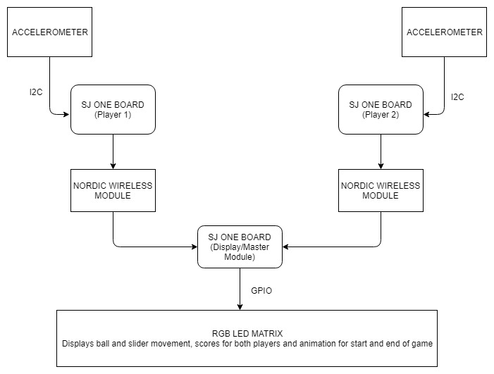
This project involves implementation of a wireless and hand-gesture controlled multiplayer ping pong (2D) game using the Adafruit's 16x32 RGB LED Matrix. It incorporates the on-board RF Nordic wireless transceiver for wireless communication and the on-board acceleration sensor to translate the hand movement into the slider movement on the display.
Objectives & Introduction
Show list of your objectives. This section includes the high level details of your project. You can write about the various sensors or peripherals you used to get your project completed.
Team Members & Responsibilities
- Akil Khan
- Design and development of the RGB Led Matrix driver
- Game logic development, implementation, QA and testing.
- Abhilash Tuse
- Game logic development
- Logic Development for communication between hand gesture control board and controller board
- Disha Patil
- Design of PCB using Eagle for Power Supply
- Hand gesture control logic development using accelerometer
- Omkar Kale
- Hand gesture control logic development using accelerometer
- Logic Development for communication between hand gesture control board and controller board
- Vishal Shrivastava
- Design and development of the RGB Led Matrix driver
- Design of PCB using Eagle for Power Supply
Schedule
Show a simple table or figures that show your scheduled as planned before you started working on the project. Then in another table column, write down the actual schedule so that readers can see the planned vs. actual goals. The point of the schedule is for readers to assess how to pace themselves if they are doing a similar project.
| Week# | Date | Task | Status | Actual Completion Date |
|---|---|---|---|---|
| 1 | 04/10/2018 |
|
|
|
| 2 | 04/17/2018 |
|
|
|
| 3 | 04/24/2018 |
|
|
|
| 4 | 05/01/2018 |
|
|
|
| 5 | 05/08/2018 |
|
|
|
| 6 | 04/15/2018 |
|
|
|
Parts List & Cost
| Item# | Part | Manufacturer | Part number | Quantity | Cost($) |
|---|---|---|---|---|---|
| 1 | SJ One Board | Preet | 3 | 80.00 | |
| 2 | Adafruit RGB LED Matrix | LED Matrix | 1 | 35.00 | |
| 3 | Power Adapter | Power Supply | 1 | 7.95 | |
| 4 | Power Bank 800mah | Aibocn | 2 | 11.95 | |
| 5 | PCB Board | ||||
| 6 | Hardware | Excess Solution | Barrel Jack, Jumper wires, Connectors | 5.00 |
- Total Cost:306.955$
Design & Implementation
The design section can go over your hardware and software design. Organize this section using sub-sections that go over your design and implementation.
Hardware Design
Accelerometer
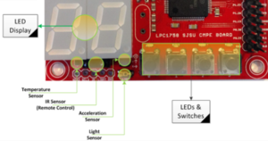
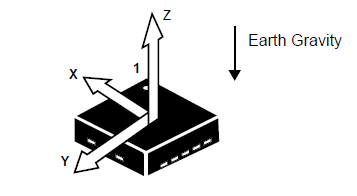
The SJOne board has an accelerometer which is interfaced on the I2C2 bus. Accelerometers are electromechanical devices that sense either static or dynamic forces of acceleration. Static forces include gravity, while dynamic forces can include vibrations and movement.The measurements are on 3-axis and these values can be calibrated to find the desired values.
In our project, accelerometer is used for detecting the up-down movement of the wrist. We are using accelerometers on two SJ-One Boards for gesture recognition. The movement from accelerometer sensor will be used to control the slider movement on the RGB LED Matrix.
Wireless Module
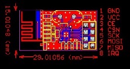
Nordic wireless chip nRF24L01+ is interfaced with SJone board using SPI bus protocol.
The nRF24L01+ is a single chip 2.4GHz transceiver with an embedded baseband protocol engine, suitable for ultra low power wireless applications. The nRF24L01+ is designed for operation in the frequency band of 2.400 - 2.483GHz. The high air data rate combined with two power saving modes make the nRF24L01+ very suitable for ultra low power designs. The nRF24L01 integrates a complete 2.4GHz RF transceiver, RF synthesizer, and baseband logic including the Enhanced ShockBurst™ hardware protocol accelerator supporting a high-speed SPI interface for the application controller. No external loop filter, resonators, or VCO varactor diodes are required, only a low-cost ±60ppm crystal, matching circuitry, and antenna.
RGB LED Matrix
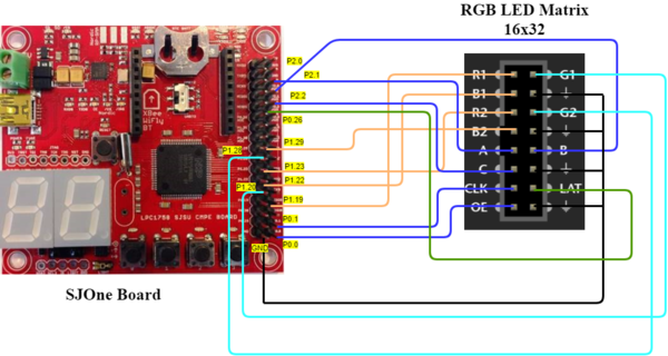
Pin mapping of RGB LED matrix with SJ One board:
| RGB LED matrix Pins | SJ One Board Pins | Function |
|---|---|---|
| R1 | P1.19 | Red Data top half |
| G1 | P1.20 | Green Data top half |
| B1 | P1.22 | Blue Data top half |
| R2 | P1.23 | Red Data bottom half |
| G2 | P1.28 | Green Data bottom half |
| B2 | P1.29 | Blue Data bottom half |
| A | P2.0 | Row select A |
| B | P2.1 | Row select B |
| C | P2.2 | Row select C |
| CLK | P0.1 | The CLK (clock) signal marks the arrival of each bit of data. |
| OE | P0.0 | OE (output enable) switches the LEDs off when transitioning from one row to the next. |
| LAT | P0.26 | The LAT (latch) signal marks the end of a row of data. |
Hardware Interface Diagram
In this section, you can describe how your hardware communicates, such as which BUSes used. You can discuss your driver implementation here, such that the Software Design section is isolated to talk about high level workings rather than inner working of your project.
Eagle Schematic
The PCB Layout is designed using the Eagle Software v8.7.1. Board consists of 2 power supplies which are powering:
- SJone board (5V, 500mA)
- RGB LED Matrix (5V,2A)
The Power Supply circuit has an LM317 voltage regulator IC and a voltage divider to fulfill the specific power requirements. The circuit was simulated using MultiSim v14.1 software by NI (National Instruments).
Printed Circuit Board also has provisions for the connection of the SJone pin headers and RGB LED Matrix's connector. The connections are as shown in the hardware description diagram.
Software Design
Show your software design. For example, if you are designing an MP3 Player, show the tasks that you are using, and what they are doing at a high level. Do not show the details of the code. For example, do not show exact code, but you may show psuedocode and fragments of code. Keep in mind that you are showing DESIGN of your software, not the inner workings of it.
RGB LED Matrix
These 16x32 5V,2A supply RGB LED Matrix panels require 12 digital pins (6 bit data, 6 bit control). They have 512 bright RGB LEDs arranged in a 16x32 grid on the front. These displays are 'chainable' - connect output to the next input. This display requires about 800 bytes of RAM to buffer the 12-bit color image. As the matrix panel has a 6-bit parallel interface, SPI hardware won't help and hence simple GPIO interface has been used to communicate with the RGB LED Matrix. As these displays don't have built-in PWM control of any kind, the driver is supposed to redraw the screen over and over to 'manually' PWM the whole thing.
Pins R1, G1 and B1 deliver data to the top half of the display whereas R2, G2 and B2 deliver data to the bottom half of the display. Pins A, B, C and D select which two rows of the display are currently lit. The LAT signal acts as the strobe and marks the end of a row of data. The CLK signal marks the arrival of each bit of data. OE (output enable) is an active low signal that switches the LEDs off when transitioning from one row to the next.
Implementation consists of 768 byte buffer for storing the pixel values for all LEDs on the display. Every line is scanned and the values for the pixels are updated every 1 ms. Between every transition of the clock from low to high, the values for the pixels are updated. As the screen is refreshed and updated very frequently, it gives the impression of a moving image.
Hand Gesture Control Logic
Implementation
This section includes implementation, but again, not the details, just the high level. For example, you can list the steps it takes to communicate over a sensor, or the steps needed to write a page of memory onto SPI Flash. You can include sub-sections for each of your component implementation.
Testing
Module testing
Acceleration Measurement
Hand gesture recognition was rigorously tested. The values received from accelerometer sensor were within a range. So, we had to test the range of values received at which the slider on screen looked responsive and smooth. We tested values ranging from -1000 to +1000 to find the right range of values. The hand gesture module transmits uint8_t. So, we checked whether the output at minimum and maximum input values was within valid range. We also checked the uint8_t value(index) transmitted depending upon the inputs received from the accelerometer sensor.
LCD Display
Integration testing
PCB Testing
The PCB was tested by checking the connectivity of the path on the copper clad tracks using a Digital Multimeter. The circuit on the PCB was simulated using MultiSim v14.1 Software and results were verified on the actual board. All the connector-related bugs were fixed by inspection and drilling the PCB wherever necessary. The board was tested for any short circuit by checking the connectivity between the Supply tracks and common ground tracks.
Technical Challenges
PCB Designing
Task Synchronization Issue
RGB LED Matrix Refresh Issue
Conclusion
Conclude your project here. You can recap your testing and problems. You should address the "so what" part here to indicate what you ultimately learnt from this project. How has this project increased your knowledge?
Project Video
Upload a video of your project and post the link here.
Project Source Code
References
Acknowledgement
We would like to thank our Professor Preetpal Kang for all his teachings and inspirational lectures. Not only did we enjoy working though out this project but also gave us an overall learning experience and precious life lessons. We would also like to thank the ISA members for always being ready to help with whatever issues we faced.
References Used
[1] FreeRTOS documentations [2] Adafruit LCD library [3] CMPE 244 Lecture notes from Preetpal Kang, Computer Engineering, San Jose State University. Feb - May 2018. [4] Nordic wireless datasheet
