S13: Door Alarm System
Contents
Door Alarm System
Abstract
Our project is a alarm system that will allow the user to lock/unlock a door simply by sending a text message. An RFID module will also be implemented as an alternative to opening the door. The user can receive a text message or phone call from the system about the current status of the door. The purpose for this project is to improve security as well as allowing easier access for people who are tired of using the traditional key.
Objectives & Introduction
- System will lock or unlock base on the message sent by the user
- If door scans an RFID tag
- Tags with correct code will have access
- System will send text message that a correct tag has been scanned.
- System will have function to call user's phone
Team Members & Responsibilities
Thanh Huynh
- Design and creating FreeRTOS task for:
- Communication with GSM
- Sending and reciveing SMS message
- Making phone call
- Reading RFID tags
- Processing information and passing it to GSM
- Interfacing with servo
- Interfacing with LCD
- Communication with GSM
Phi Le
- Drivers Development for:
- Both UART2 and UART3 driver
- Pulse width modulation (PWM)
- Interfacing servo to board
- Hardware construction of system
- Assisted and gave input in trouble shooting
Schedule
| Week Number | Planned Tasks | Actual Tasks |
|---|---|---|
| Week 1
|
|
|
| Week 2
|
|
|
| Week 3
|
|
|
| Week 4
|
|
|
| Week 5
|
|
|
Parts List & Cost
| Parts | Cost |
|---|---|
| 2012 SJ One Board | $40 |
| RFID Complete Kit | $50 |
| Jumper Wires | $6 |
| SD Card 16gb | $10 |
| NewHaven LCD | $25 |
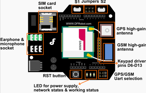
| GSM/GPS Module V3 | $89 |
| Piezo Buzzer | $1 |
| Servo | $15 |
| Total: | $236 |
Design & Implementation
Hardware Design
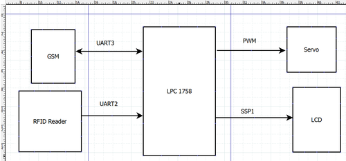
The entire hardware block diagram is shown below
The entire hardware block diagram is shown below
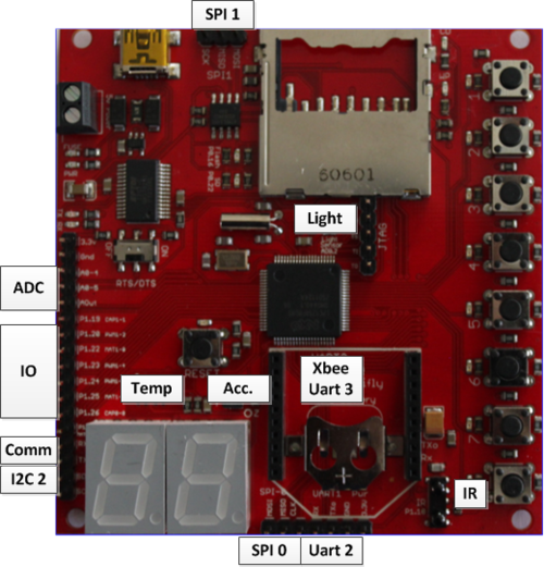
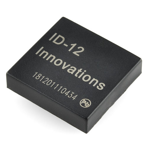
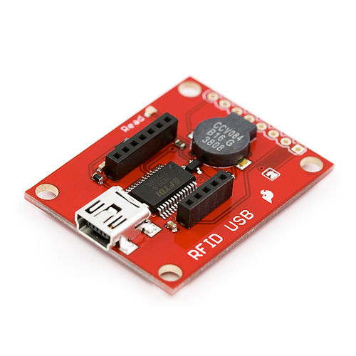
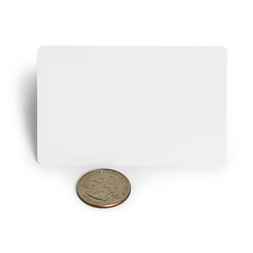
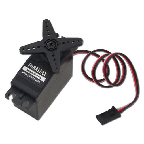
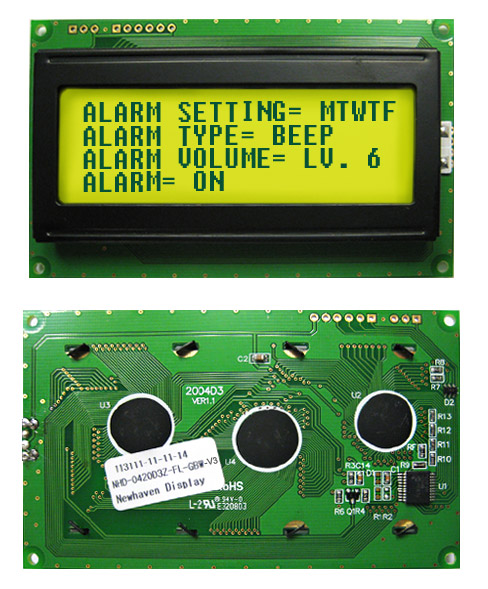
The heart of the system is the micro-controller LPC1758 integrated to the SJ One board. It controls all components in the system such as RFID reader, GSM module, servo and LCD through UART, PWM and SPI interfaces.
The following are individual components of the system
Hardware Interface
In this section, you can describe how your hardware communicates, such as which BUSes used. You can discuss your driver implementation here, such that the Software Design section is isolated to talk about high level workings rather than inner working of your project.
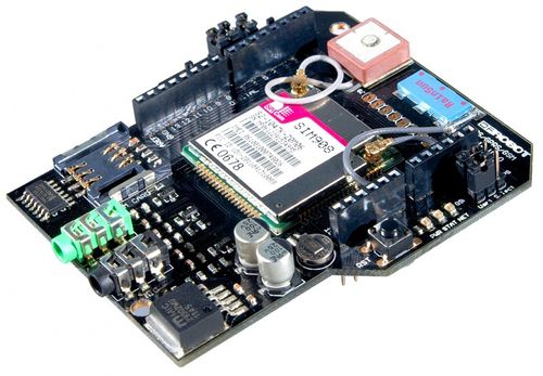
This GSM module will allow us to send and receive messages from our phone. This GSM module was designed to be compatatible with an Arduino Revision 3 board. However this board can be connected to the SJ ONE board using UART2 for communication. Connect RX pin from UART2 to TX pin from GSM. Connect TX pin from UART2 to TX pin of GSM. This GSM module requires a baud rate of 38400 bits per seconds.
Software Design
Show your software design. For example, if you are designing an MP3 Player, show the tasks that you are using, and what they are doing at a high level. Do not show the details of the code. For example, do not show exact code, but you may show psuedocode and fragments of code. Keep in mind that you are showing DESIGN of your software, not the inner workings of it.
How to Send a Message
Steps:
1. Send:AT
2. Send:At+CMGF=1
3. Send:AT+CMGS="XXXXXXXXXX" (X means phone number of the receiver)
4. wait for indicator '<' and start typing your message
5. when done Send character 'ctrl+z'
How to Make a phone Call
Steps:
1. Send:AT
2. Send:ATDXXXXXXXXXX; (X means receiver's phone number, then end with a semicolon);
Above are steps of how to send AT command through serial communication. For example in order to make a phone call, first send string 'AT' to the GSM. GSM will reply with AT which will acknowledge that it received your command. Then proceed by sending "ATD" concatenated with a phone number. It will take a few seconds for the GSM to establish a connection before calling the phone number. After the receiver hangs up the phone the GSM will send a message through serial indicating phone call has ended.
Implementation
This section includes implementation, but again, not the details, just the high level. For example, you can list the steps it takes to communicate over a sensor, or the steps needed to write a page of memory onto SPI Flash. You can include sub-sections for each of your component implementation.
Testing & Technical Challenges
Describe the challenges of your project. What advise would you give yourself or someone else if your project can be started from scratch again? Make a smooth transition to testing section and described what it took to test your project.
Include sub-sections that list out a problem and solution, such as:
- Could not establish serial communication with GSM module v3
- GSM jumpers need to be in correct location. The following switch configuration needs to be established on the board in order to send or receive AT commands. Switch 1: USB, Switch 2: Comm, Switch 3: GSM.
- Uart is is not working properly, sometimes it work and sometimes is does not.
- All ground wires need to be connected together in order to establish a common GROUND.
- GSM module is not sending back any acknowledgement signal or is not processing any AT command that I am sending to it.
- A newline character 'r' is required after most AT command sent to GSM.
- Sometime a delay is required before the next AT command can be sent.
Wifi Connection Issues
Many wifi connection issues were encountered. To solve this problem, a dedicated task was created to re-connect to wifi if the connection was ever lost.
Conclusion
Conclude your project here. You can recap your testing and problems. You should address the "so what" part here to indicate what you ultimately learnt from this project. How has this project increased your knowledge?
Project Video
Upload a video of your project and post the link here.
Project Source Code
Send me your zipped source code and I will upload this to SourceForge and link it for you.
References
Acknowledgement
Any acknowledgement that you may wish to provide can be included here.
References Used
List any references used in project.
- DFROBOT's Wiki:http://www.dfrobot.com/wiki/index.php/GPS/GPRS/GSM_Module_V3.0_(SKU:TEL0051)
- SIM908 AT Command Manual_V1.01
- RFID ID-12 Data sheet
Appendix
You can list the references you used.
