Difference between revisions of "F20: Corona Run"
Proj user4 (talk | contribs) (→Hardware Interface) |
Proj user4 (talk | contribs) (→Hardware Interface) |
||
| Line 186: | Line 186: | ||
=== Hardware Interface === | === Hardware Interface === | ||
| − | |||
| − | |||
'''Our Approach to LED Matrix:''' | '''Our Approach to LED Matrix:''' | ||
| Line 212: | Line 210: | ||
Gnd - Ground (0V) | Gnd - Ground (0V) | ||
| + | |||
| + | |||
| + | [[File:FIG-Intro to LED Matrix.GIF|575px| thumb| centre |Introduction to LED ]] | ||
The RGB LED Display Matrix gets the input from Master Module which is our SJTwo board. It is driven by the GPIO Pins of the Master Module. However, these GPIO pins are not connected directly to the display matrix since 64x64 RGB LED Matrix drives on 5V input whereas the GPIO pins from SJTwo board output 3.3V. So, two level shifter ICs are used as an intermediate connection to convert 3.3V GPIO output from SJTwo board to 5V before giving it as an input to the RGB Led Matrix. Each LED can be independently addressed and controlled. This 64x64 LED matrix has 5 address lines viz. A, B, C, D, E. With 5 address lines, we get 2^5 = 32 unique addresses. But, the matrix has 64 rows. The scan rate of the LED Matrix is 1/32, i.e., 2/64. This indicates that by making each address line high, two rows will be driven at the same time. As shown R1,G1,B1 handles the section 1 of the LED Matrix and R2,G2,B2 handles the section 2 of the matrix. | The RGB LED Display Matrix gets the input from Master Module which is our SJTwo board. It is driven by the GPIO Pins of the Master Module. However, these GPIO pins are not connected directly to the display matrix since 64x64 RGB LED Matrix drives on 5V input whereas the GPIO pins from SJTwo board output 3.3V. So, two level shifter ICs are used as an intermediate connection to convert 3.3V GPIO output from SJTwo board to 5V before giving it as an input to the RGB Led Matrix. Each LED can be independently addressed and controlled. This 64x64 LED matrix has 5 address lines viz. A, B, C, D, E. With 5 address lines, we get 2^5 = 32 unique addresses. But, the matrix has 64 rows. The scan rate of the LED Matrix is 1/32, i.e., 2/64. This indicates that by making each address line high, two rows will be driven at the same time. As shown R1,G1,B1 handles the section 1 of the LED Matrix and R2,G2,B2 handles the section 2 of the matrix. | ||
Revision as of 19:22, 16 December 2020
Contents
Corona Run
Abstract
CORONA Run is a game designed for every one (Not PG-13 Rated) to have a good time during this pandemic. Inspired by the current real-life pandemic situation and the game "Minion Rush", the main objective of this game is to avoid CORONA virus. As the game progresses, the player will encounter not only the virus, but also power-ups that provide the player with temporary immunity to the virus. The score of the player will depend on how long the player can survive the game.
Objectives & Introduction
The main objective of this project is to use SJ2 board as the center of our project. To create a properly working game, the game must be able to:
- Detect collision with CORONA virus to end the game
- Provide the player with power-ups when the player touches it
- Keep track of the score
There are some requirements that must be used when creating the game, such as:
- Utilizing FreeRTOS to run the game on SJ2 Board
- Utilizing accelerometer to control the game
Team Members & Responsibilities
Schedule
| Week | Date | Task | Actual |
|---|---|---|---|
| 1 | 09/16 |
|
|
| 2 | 09/18 |
|
|
| 3 | 09/26 | Project Proposal Submission | Completed |
| 4 | 10/13 |
|
|
| 5 | 10/19 |
|
|
| 6 | 10/23 |
|
|
| 7 | 10/25 |
|
|
| 8 | 10/30 |
|
|
| 9 | 11/1 - 11/7 |
|
|
| 10 | 11/8 - 11/14 |
|
|
| 11 | 11/15 - 11/28 |
|
|
| 12 | 11/29 - 12/5 |
|
|
| 13 | 12/6 - 12/12 |
|
|
| 14 | 12/15 |
|
|
Parts List & Cost
Give a simple list of the cost of your project broken down by components. Do not write long stories here.
Design & Implementation
The design section can go over your hardware and software design. Organize this section using sub-sections that go over your design and implementation.
Hardware Design
Discuss your hardware design here. Show detailed schematics, and the interface here.
Hardware Interface
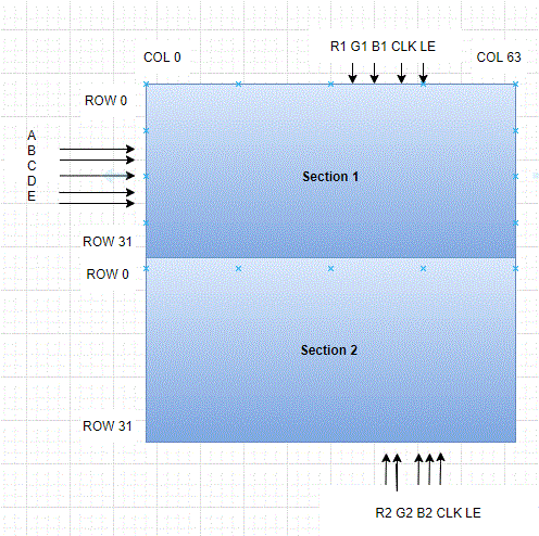
Our Approach to LED Matrix: We have divided LED display Matrix into two sections
Section 1 - First 32 rows (Row 0 to row 31) Section 2 - Remaining 32 rows (Row 32 to row 63)
There are 6 data lines, 3 for each section are available to drive the RGB matrix.
Section 1: R1, G1, B1
Section 2. R2, G2 , B2
Other pins:
OE - Output Enable
Lat - Latch
Clk - clock signal
Vcc - High Voltage (5V)
Gnd - Ground (0V)
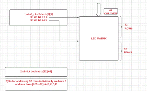
The RGB LED Display Matrix gets the input from Master Module which is our SJTwo board. It is driven by the GPIO Pins of the Master Module. However, these GPIO pins are not connected directly to the display matrix since 64x64 RGB LED Matrix drives on 5V input whereas the GPIO pins from SJTwo board output 3.3V. So, two level shifter ICs are used as an intermediate connection to convert 3.3V GPIO output from SJTwo board to 5V before giving it as an input to the RGB Led Matrix. Each LED can be independently addressed and controlled. This 64x64 LED matrix has 5 address lines viz. A, B, C, D, E. With 5 address lines, we get 2^5 = 32 unique addresses. But, the matrix has 64 rows. The scan rate of the LED Matrix is 1/32, i.e., 2/64. This indicates that by making each address line high, two rows will be driven at the same time. As shown R1,G1,B1 handles the section 1 of the LED Matrix and R2,G2,B2 handles the section 2 of the matrix.
| Sr. No. | SJTwo board Pin | LED MATRIX | Function |
|---|---|---|---|
| 1 | P1_31 | R1 | Upper half (Section 1) |
| 2 | P1_30 | G1 | Upper half (Section 1) |
| 3 | P1_23 | B1 | Upper half (Section 1) |
| 4 | P1_28 | R2 | Lower half (Section 2) |
| 5 | P1_29 | G2 | Lower half (Section 2) |
| 6 | P2_0 | B2 | Lower half (Section 2) |
| 7 | P2_2 | A | Address Line |
| 8 | P2_4 | B | Address Line |
| 9 | P2_5 | C | Address Line |
| 10 | P2_6 | D | Address Line |
| 11 | P2_0 | E | Address Line |
| 12 | P2_7 | Clk | For upper half and lower half |
| 13 | P2_8 | Latch | For upper half and lower half |
| 14 | P2_9 | OE | For upper half and lower half |
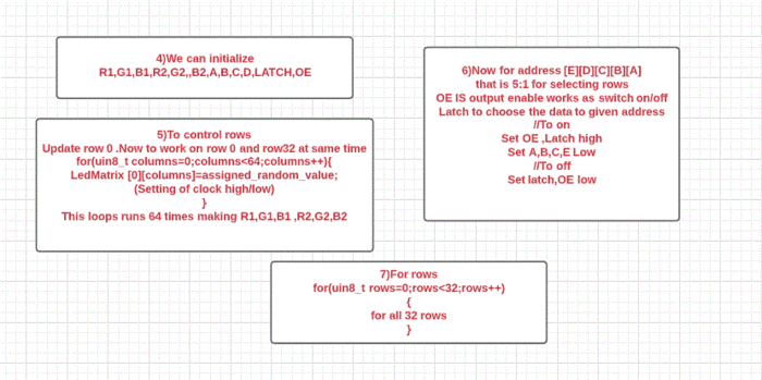
The row contains 5:32 decoder as shown in the figure .Here the rows are selected in parallel so if row 1 starts functioning then simultaneously 33 will start .There are five address which are marked as A,B,C,D,E ,only one input is active low at time .The pseudo code is presented below to give broad description how the row can be operated on LED matrix .
The column data is stored in a 64-bit serial-in, a parallel-out shift register. The shift register is designed to work with LEDs and implements a constant-current system that ensures the LED brightness remains uniform.R1,G1,B1 is for section 1 32x64 and R2,G2,B2 is for section 2 .There is single clock interfaced between them. Once the clocking and shifting the register is completed . We need to latch this data to the register. The register data is sent out to all the row lines and that Row line which is pulled low by the decoder will receive this data and corresponding pixels are turned on. The pseudo code is presented below to give broad description how the column can be operated on LED matrix .
Software Design
Show your software design. For example, if you are designing an MP3 Player, show the tasks that you are using, and what they are doing at a high level. Do not show the details of the code. For example, do not show exact code, but you may show psuedocode and fragments of code. Keep in mind that you are showing DESIGN of your software, not the inner workings of it.
Implementation
This section includes implementation, but again, not the details, just the high level. For example, you can list the steps it takes to communicate over a sensor, or the steps needed to write a page of memory onto SPI Flash. You can include sub-sections for each of your component implementation.
Testing & Technical Challenges
Describe the challenges of your project. What advise would you give yourself or someone else if your project can be started from scratch again? Make a smooth transition to testing section and described what it took to test your project.
Include sub-sections that list out a problem and solution, such as:
<Bug/issue name>
Discuss the issue and resolution.
Conclusion
Conclude your project here. You can recap your testing and problems. You should address the "so what" part here to indicate what you ultimately learnt from this project. How has this project increased your knowledge?
Project Video
Upload a video of your project and post the link here.
Project Source Code
References
Acknowledgement
We would like to acknowledge the open source software community, which provided us with Audacity. We also would like to acknowledge the creators of the free-to-use sound effects we used. Thank you!
References Used
MMA8452Q datasheet (Sparkfun)
Adafruit Sound FX Sound Board pinouts
Converting sound files with Audacity
Wiki formatting
Appendix
You can list the references you used.


