Difference between revisions of "F19: Tetris"
Proj user1 (talk | contribs) (→SJTwo Micro-controller to LED Matrix Pin Connections) |
Proj user1 (talk | contribs) (→Power Circuit) |
||
| Line 310: | Line 310: | ||
=== Power Circuit === | === Power Circuit === | ||
| − | + | The initial design of the PCB power circuit was to power one micro-controller and the led matrix. The power circuit consists of a barrel jack connector(labeled JACK as shown in the schematic below) connected to a 5V voltage regulator. The voltage regulator Vin and Vout terminals are connected to capacitors to avoid potential voltage spikes which may result in damage to any connected hardware that ideally operated up to 5V. | |
[[File:TET_schematic.png | 450px |''' Schematic of for PCB Design ''']] | [[File:TET_schematic.png | 450px |''' Schematic of for PCB Design ''']] | ||
Revision as of 01:18, 16 December 2019
Contents
Grading Criteria
(Take out Later)
- How well is Software & Hardware Design described?
- How well can this report be used to reproduce this project?
- Code Quality
- Overall Report Quality:
- Software Block Diagrams
- Hardware Block Diagrams
- Schematic Quality
- Quality of technical challenges and solutions adopted.
Project Title
LED Matrix Tetris
Abstract
Our project is creating the game of Tetris using the LED matrix as our display and creating the driver for the game using the SJSU2 board from the class.
Objectives & Introduction
Show list of your objectives. This section includes the high level details of your project. You can write about the various sensors or peripherals you used to get your project completed.
Team Members & Main Responsibilities
| Administrative Roles | ||||
|---|---|---|---|---|
|
Kevin Chan & Lawrence Wan | |||
|
Kevin Chan | |||
|
Yuming Cheng | |||
|
Yuming Cheng | |||
|
Lawrence Wan & Kevin Chan | |||
Technical Responsibilities
| Technical Responsibilities | ||||
|---|---|---|---|---|
|
Kevin Chan & Lawrence Wan & Yuming Cheng | |||
|
Kevin Chan | |||
|
Yuming Cheng & Lawrence Wan | |||
|
Lawrence Wan | |||
|
James Ding & Lawrence Wan | |||
Schedule
Show a simple table or figures that show your scheduled as planned before you started working on the project. Then in another table column, write down the actual schedule so that readers can see the planned vs. actual goals. The point of the schedule is for readers to assess how to pace themselves if they are doing a similar project.
Team Deliverables Schedule
| WEEK |
START DATE |
END DATE |
TASK DETAILS |
STATUS |
|---|---|---|---|---|
| 1 | 8 Oct 2019 | 21 Oct 2019 |
Create and establish GitLab repository |
Complete Complete Complete Complete Complete Complete |
| 2 | 22 Oct 2019 | 4 Nov 2019 |
Create a Bill of Materials. |
In Progress Complete In progress |
| 3 | 5 Nov 2019 | 11 Nov 2019 |
Finalize the Wiki schedule for submission |
In progress Complete (Basic function complete) In Progress (working on rotation) |
| 4 | 12 Nov 2019 | 18 Nov 2019 |
Received the PCB and start working on connections |
In progress ( Waiting for PCB ) In progress In progress In progress In progress |
| 5 | 19 Nov 2019 | 25 Nov 2019 |
Starting to assemble the enclosing |
Waiting for Materials In progress In progress Not Started Not Started (Debating accordingly to our progress) |
| 6 | 26 Nov 2019 | 2 Dec 2019 |
Polishing the Hardware and Software for project. |
Not Started Not Started Not Started In progress |
| 7 | 3 Dec 2019 | 9 Dec 2019 |
FIELD TESTING - CRITICAL WEEK |
Not Started Not Started Not Started Not Started |
| 8 | 10 Dec 2019 | 17 Dec 2019 |
All hands on testing and final bug fixes. |
Not Started Not Started Not Started Not Started |
| Final | 18 Dec 2019 |
DEMO: Final Project |
In progress In progress |
Parts List & Cost
Give a simple list of the cost of your project broken down by components. Do not write long stories here.
| PART NAME |
PART MODEL & SOURCE |
QUANTITY |
COST (USD) |
|---|---|---|---|
|
|
|
|
|
|
|
|
|
|
|
|
|
|
|
|
|
|
|
|
|
|
|
|
|
|
|
|
|
|
|
|
|
|
|
|
|
|
|
|
|
|
|
|
| Total Cost: |
|
Design & Implementation
The design section can go over your hardware and software design. Organize this section using sub-sections that go over your design and implementation.
Hardware Design
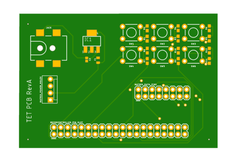
The PCB design began with the primary objective of interfacing the SJTwo micro-controller with the LED Matrix Display with ease. Initially, the second objective was to create a power circuit to power the SJTwo micro-controller and led matrix, however, later decisions have led to re-purposing the circuit post-manufacturing of the PCB. The third objective was to create circuits for external buttons to operate the game.
SJTwo Micro-controller to LED Matrix Pin Connections
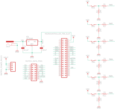
Interfacing the microcontroller and matrix with ease meant avoiding the use of loose wiring as much as possible. Since the matrix itself came with a ribbon cable, it was decided that we design the PCB around using the ribbon cable to interface it with the micro-controller. It was decided to slot the PCB with the micro-controller with 2x40 through-hole headers (labeled as MICROCONTROLLER_PIN_SLOT in the schematic below). The pre-selected pins needed from the micro-controller to interface with the matrix are then connected to 2x8 header pins (labeled as MATRIX_DATA_PINS) which correspond to the pinout of the 32x32 LED Matrix data pins.
Power Circuit
The initial design of the PCB power circuit was to power one micro-controller and the led matrix. The power circuit consists of a barrel jack connector(labeled JACK as shown in the schematic below) connected to a 5V voltage regulator. The voltage regulator Vin and Vout terminals are connected to capacitors to avoid potential voltage spikes which may result in damage to any connected hardware that ideally operated up to 5V.
Hardware Interface
In this section, you can describe how your hardware communicates, such as which BUSes used. You can discuss your driver implementation here, such that the Software Design section is isolated to talk about high level workings rather than inner working of your project.
Configuration of the 32x32 LED Matrix
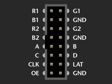
The 32x32 LED matrix was purchased from Adafruit. The pinout diagram below shows the pins that are needed to be interfaced with SJTwo Microcontroller. Descriptions of each of the pins are provided in the following sections. The most straight forward of the pins below is ground, where each of the ground pins were connected to a ground plane on the PCB where it was grounded with the SJTwo board.
R1,R2,G1,G2,B1,B2
R1,R2,G1,G2,B1,B2, correspond to the color (Red, Green, Blue) that will be shifted in the shift register that will be displayed onto the LED matrix. On our display, the colors are shifted in from left to right. The number associated with each pin, determines if it is on the top or bottom half of the display. For example, if R1, B1 and G1, are set to high, then the output color will be white. GPIO pins from the SJTwo board were used to configure these pins to control color. To reduce the amount of clock cycles to draw an image, we draw both top and bottom images at the same time. More explanation of this is seen below.
A B C D
A, B, C, D, pins correspond to the addressing of each row that the colors R1,R2,G1,G2,B1,B2 will be written to.
The figure and table below shows the pin-out of RGB LED matrix with description.
| Label | Name | Function | Pin Connection |
|---|---|---|---|
| 1 | R1 | High R data | Pin 2.2 |
| 2 | G1 | High G data | Pin 2.4 |
| 3 | B1 | High B data | Pin 2.5 |
| 4 | R2 | Low R data | Pin 2.6 |
| 5 | G2 | Low G data | PIn 2.7 |
| 6 | B2 | Low B data | PIn 2.8 |
| 7 | A | A line selection | Pin 1.31 |
| 8 | B | B line selection | Pin 1.30 |
| 9 | C | C line selection | Pin 1.20 |
| 10 | D | D line selection | Pin 1.23 |
| 11 | CLK | CLOCK | Pin 2.0 |
| 12 | LAT | LATCH | Pin 2.1 |
| 13 | OE | Output Enable | Pin 0.17 |
| 14 | GND | GND | Pin GND |
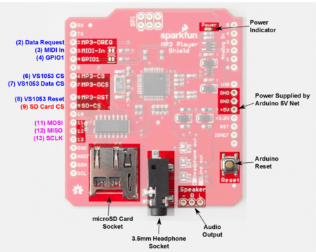
Interfacing with the VS1053 MP3 Decoder

| Label | Name | Function | Pin Connection |
|---|---|---|---|
| 1 | MP3-DREQ | Decoder Data Request | Pin 0.1 |
| 2 | MP3-CS | VS1053 Chip Select | Pin 0.22 |
| 3 | MP3-DCS | VS1053 Data CS | Pin 0.0 |
| 4 | MP3-RST | VS1053 Reset | Pin 0.18 |
| 5 | MOSI | SPI Bus (Master Output Slave Input) | Pin 0.9 |
| 6 | MISO | SPI Bus (Master Input Slave Output) | Pin 0.8 |
| 7 | SCK | SPI Clock | Pin 0.7 |
| 8 | +5V | +5V | PCB Vout |
| 9 | GND | GND | GND |
Software Design
Show your software design. For example, if you are designing an MP3 Player, show the tasks that you are using, and what they are doing at a high level. Do not show the details of the code. For example, do not show exact code, but you may show psuedocode and fragments of code. Keep in mind that you are showing DESIGN of your software, not the inner workings of it.
Implementation
This section includes implementation, but again, not the details, just the high level. For example, you can list the steps it takes to communicate over a sensor, or the steps needed to write a page of memory onto SPI Flash. You can include sub-sections for each of your component implementation.
Testing & Technical Challenges
Describe the challenges of your project. What advise would you give yourself or someone else if your project can be started from scratch again? Make a smooth transition to testing section and described what it took to test your project.
Include sub-sections that list out a problem and solution, such as:
<Bug/issue name>
Discuss the issue and resolution.
Conclusion
Conclude your project here. You can recap your testing and problems. You should address the "so what" part here to indicate what you ultimately learnt from this project. How has this project increased your knowledge?
Project Video
Upload a video of your project and post the link here.
Project Source Code
- Sourceforge Source Code Link //preet wbsite example take out later
- GitLab for Source Code
References
Acknowledgement
Any acknowledgement that you may wish to provide can be included here.
References Used
List any references used in project.
Appendix
You can list the references you used.


