Difference between revisions of "F20: Flappy"
Proj user2 (talk | contribs) (→Obstacles Generations) |
Proj user2 (talk | contribs) (→Hardware Design) |
||
| Line 193: | Line 193: | ||
=== Hardware Design === | === Hardware Design === | ||
* PCB Goals | * PCB Goals | ||
| − | A PCB is developed to simplify component connections by completely removing the use of jumper cables providing a compact design with solid connections. With this in mind, our team immediately wanted to move over to ribbon cables for both the SJ2 and LED matrix. The SJ2 board also connects to two coprocessing boards: the audio and amplifier Adafruit. These boards can connect directly onto the PCB using female headers acting like a "hat" for the PCB. See assembled PCB picture to see the final outcome of the PCB, otherwise read-on for more information on the board! | + | A PCB is developed to simplify component connections by completely removing the use of jumper cables providing a compact design with solid connections. With this in mind, our team immediately wanted to move over to ribbon cables for both the SJ2 and LED matrix. The SJ2 board also connects to two coprocessing boards: the audio and amplifier by Adafruit. These boards can connect directly onto the PCB using male-to-female headers acting like a "hat" for the PCB. The PCB also provides a hardware solution for debouncing the big switch that is used in this project. See assembled PCB picture at the end of this section to see the final outcome of the PCB, otherwise read-on for more information on the design of the board! |
[[File:Flappy_schematic.png|thumb|center|500px|''' Schematic ''']] | [[File:Flappy_schematic.png|thumb|center|500px|''' Schematic ''']] | ||
| Line 282: | Line 282: | ||
|} | |} | ||
| − | + | * Schematic and Pinout | |
| − | * | + | Provided above is the schematic and connections mapping table. Starting with jumpers: J1 is the 5V Jack Barrel Adapter connection, J2 is the 2x20 shrouded ribbon cable connector for the SJ2 board, J3 is the 2x8 shrouded ribbon cable connector for the LED matrix GPIOs, J4 is the molex power connector for the RGB LED matrix, and J5 is where the big switch is connected for the RC debouncing circuit (see Input Button and Debouncing Issue section below for more information on this circuit). All of the capacitors labelled C1 to C7 are decoupling capacitors at 100 nF with the aim of removing noise induced by connecting wires and traces a signal travels on. With this in mind, decoupling capacitors are placed very close to the voltage input of a component to provide maximum filtering effect! R1 is a 10k Ohm resistor and R2 is a 1k Ohm resister wehere both are used alongside C5 for fixing the switch debouncing issue described beforehand. Lastly, the audio board is labelled as Audio FX board and the amplifier board is labelled as MAX98306. The PCB uses a total of 19 GPIOs from the SJ2 board. The 5V Jack Barrel Adapter powers on the SJ2 board and the LED matrix. Then, the SJ2 board outputs a 3V3 output that powers both the audio and amplifier boards. |
| − | |||
| − | |||
| − | |||
| − | |||
| − | |||
| − | |||
[[File:Flappy_footprint.png|thumb|center|500px|''' Footprint''']] | [[File:Flappy_footprint.png|thumb|center|500px|''' Footprint''']] | ||
Revision as of 05:47, 18 December 2020
Contents
FLAPPY
Abstract
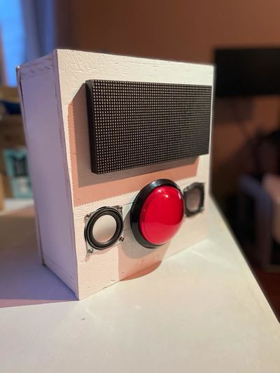
FLAPPY is one of the most anticipated gaming machines of the year 2020. Adopted the timeless design of the Gameboy Advance, it can play one and only one game(albeit the best game of all time in our opinion): FLAPPY BIRD. The player is advised to move the main character wisely (up and down) to NOT hit the beautiful green pipe. With simple gameplay and catchy music, it guarantees thousands of seconds of interesting game for the entire family.
Objectives & Introduction
The main objective of our project was to re-create the iconic Flappy Bird mobile game into a physical gaming device. Our team tried to simplify the device in accordance with the original game spirit: its simplicity. Using the SJ2 board, our team started by researching for suitable components and interfaced them together to replicate Flappy Bird
Objectives:
- Smooth button usage and it must handle the push differently based on the scenes
- Write a simple driver to communicate with the LED
- Write a separate driver for game graphic
- Design a state machine to handle different game tasks such as the start screen, gameplay, and ending screen
- Implement the game logic for movement of the bird, collision detection, randomized obstacle generation, and a score keeping system
Team Members & Responsibilities
- Huy Nguyen
- Git Admin
- LED Matrix Driver
- Game Graphic Driver
- Overall Software Stack
- Michael Wang
- LED Matrix Driver
- Obstacle Generations
- Overall Software Stack
- Brian Tran
- Soundboard Driver and Hardware Integration
- Overall Hardware Stack
- Case built and design
- Code debug
- Danny Nuch
- PCB design and Hardware Integration
- Overall Hardware Stack
- Code debug
Schedule
| Week | Date | Task | Status |
|---|---|---|---|
| 1 | 10/13 |
|
|
| 2 | 10/20 |
|
|
| 3 | 10/27 |
|
|
| 4 | 11/3 |
|
|
| 5 | 11/10 |
|
|
| 6 | 11/17 |
|
|
| 7 | 11/24 |
|
|
| 8 | 12/1 |
|
|
| 10 | 12/16 |
|
|
Parts List & Cost
| Part Name | Quantity | Cost Per Unit |
|---|---|---|
| SJ2 Board | 1 | $50 |
| 32x64 RGB LED Matrix | 1 | $22 |
| 5V Power Supply | 1 | $13.19 |
| Adafruit Soundboard | 1 | $29.95 |
| Adafruit Amplifier | 1 | $9.95 |
| Speaker | 2 | $1.95 |
| Red Button | 1 | $19.95 |
| Wood | 6 | $9.95 |
| Satin White Spray Paint | 6 | $5.98 |
Design & Implementation
Hardware Design
- PCB Goals
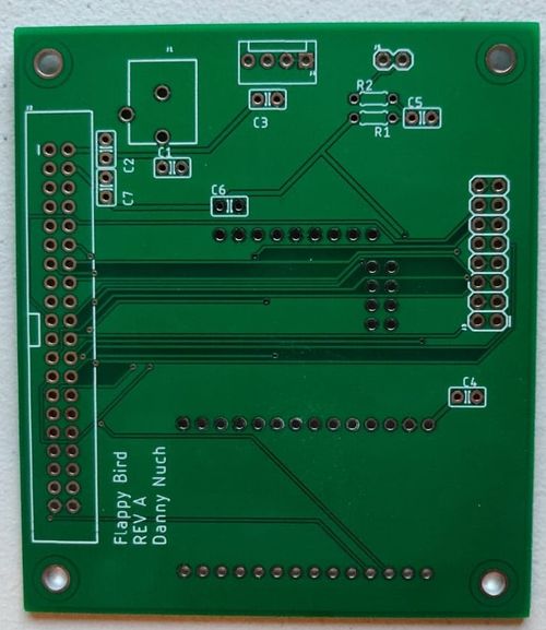
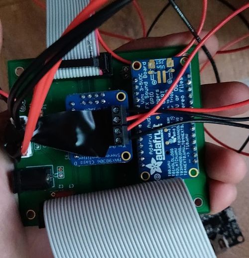
A PCB is developed to simplify component connections by completely removing the use of jumper cables providing a compact design with solid connections. With this in mind, our team immediately wanted to move over to ribbon cables for both the SJ2 and LED matrix. The SJ2 board also connects to two coprocessing boards: the audio and amplifier by Adafruit. These boards can connect directly onto the PCB using male-to-female headers acting like a "hat" for the PCB. The PCB also provides a hardware solution for debouncing the big switch that is used in this project. See assembled PCB picture at the end of this section to see the final outcome of the PCB, otherwise read-on for more information on the design of the board!
| GPIO ID number | SJ2 GPIO | Connection |
|---|---|---|
| 0 | P0.6 | Audio music connection 0 |
| 1 | P0.7 | Audio music connection 1 |
| 2 | P0.8 | Audio music connection 2 |
| 3 | P0.9 | Audio music connection 3 |
| 4 | P0.26 | Audio music connection 4 |
| 5 | P0.25 | LED matrix Red 1 |
| 6 | P1.31 | LED matrix Blue 1 |
| 7 | P1.30 | LED matrix Red 2 |
| 8 | P1.20 | LED matrix Blue 2 |
| 9 | P1.23 | LED matrix A selector |
| 10 | P1.28 | LED matrix C selector |
| 11 | P1.29 | LED matrix clock |
| 12 | P2.0 | LED matrix output enable |
| 13 | P2.1 | LED matrix Green 1 |
| 14 | P2.2 | LED matrix Green 2 |
| 15 | P2.4 | LED matrix B selector |
| 16 | P2.5 | LED matrix D selector |
| 17 | P2.5 | LED matrix Latch |
| 18 | P2.7 | Game button connection |
- Schematic and Pinout
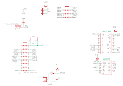
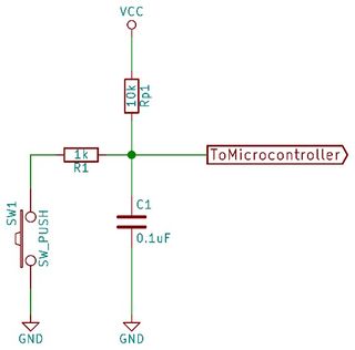
Provided above is the schematic and connections mapping table. Starting with jumpers: J1 is the 5V Jack Barrel Adapter connection, J2 is the 2x20 shrouded ribbon cable connector for the SJ2 board, J3 is the 2x8 shrouded ribbon cable connector for the LED matrix GPIOs, J4 is the molex power connector for the RGB LED matrix, and J5 is where the big switch is connected for the RC debouncing circuit (see Input Button and Debouncing Issue section below for more information on this circuit). All of the capacitors labelled C1 to C7 are decoupling capacitors at 100 nF with the aim of removing noise induced by connecting wires and traces a signal travels on. With this in mind, decoupling capacitors are placed very close to the voltage input of a component to provide maximum filtering effect! R1 is a 10k Ohm resistor and R2 is a 1k Ohm resister wehere both are used alongside C5 for fixing the switch debouncing issue described beforehand. Lastly, the audio board is labelled as Audio FX board and the amplifier board is labelled as MAX98306. The PCB uses a total of 19 GPIOs from the SJ2 board. The 5V Jack Barrel Adapter powers on the SJ2 board and the LED matrix. Then, the SJ2 board outputs a 3V3 output that powers both the audio and amplifier boards.
- Footprint Design
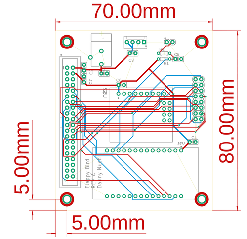
trace widths; placements of units;
- Finishing touches
qwerty
Hardware Interface
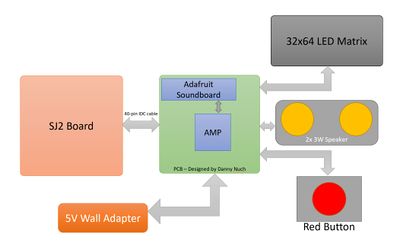
The heart of our Flappy gaming machine is the SJ2 board. The only source of input is a very Big Red Button with some serious debouncing issue (which we gladly solved it!). Base on the input and when it is being pressed, the system periodically communicate with the LED Matrix to update all the motion as well as the soundboard to play the right sound. Since we need to power so many things, the built-in 3W speakers are used with an amplifier so that we can achieve a loud and clear sound.
Adafruit Audio FX Sound Board w/ 2MB Flash
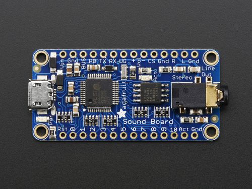
The Adafruit AudioFX board provides a simple interface to a DAC. Our variant has 2MB of flash storage and easy playback through its GPIO pin triggers. The small flash size was by choice, since loopable sounds/music in .OGG format would be compressed just enough to fit.
| AudioFX Pin | Connection |
|---|---|
| Vin | SJ2 3.3V |
| GND | Common GND |
| R | Amplifier R+ |
| L | Amplifier L+ |
| 0 | SJ2 P0.6 |
| 1 | SJ2 P0.7 |
| 2 | SJ2 P0.8 |
| 3 | SJ2 P0.9 |
| 4 | SJ2 P0.26 |
Stereo 3.7W Class D Audio Amplifier
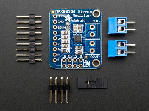
Although there is an audiofx board w/ built in amplifier, it was deteremined to be too weak. Our amplifier of choice was a standalone amplifier that can provide up to 3.7W to two different channels (L & R speakers). The amplifier also allows easy selection of gain, which we decided upon using 18dB.
| Amplifier | Connection |
|---|---|
| VDD | SJ2 3.3V |
| GND | Common GND |
| R+ | AudioFX R |
| R- | Common GND |
| L+ | AudioFX L |
| L- | Common GND |
LED Matrix Interface
To all future teams, we think it is best that you study this part from several teams to successfully implement your LED matrix. We did a lot of research as well as trial-n-errors on this type of part that has *very* little technical datasheet on it.
Our team decided to go with a 32x64 RGB LED matrix display with a 3mm pitch for the game requirements and its cost. With a scan rate of 1:32, it is sufficient for our eyes to not see glitches while the game is in play.
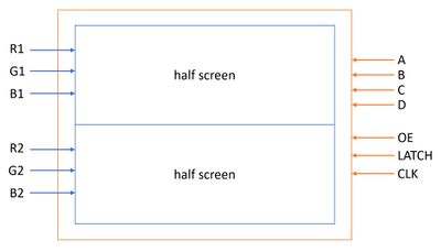
Most RGB matrix will have the same 16-pin headers and here are the main signals:
+ R1, G1, and B1
+ R2, G2, and B2
+ A, B, C, D (and possibly E in a bigger screen, or no D signal on a smaller screen)
+ Output Enable (OE)
+ LATCH
+ Clock (CLK)
+ And some ground pins
We suggest you stick with 1 LED Matrix from the same vendor and start implementing it as soon as possible. We cycled through 3 LED Matrixes in total from 2 different vendors, sticking to 1 may help reducing the amount of screen replacement should they be defective.
TIPS #1: Make sure you have a GOOD power source for your LED matrix. There are potentially “defective looking” issue with a weak power source: Lights doesn’t turn on, Lights are dimmed, etc. A decent power source will help tremendously.
Alright, we know that it’s a lot of reading but bear with us! Reading 1 guide completely will prevent you from reading 10 other guides that will lead you to nowhere.
Above is the visualization of a simple RGB LED Matrix. The most common RGB LED Matrix on the market will divide the screen into 2 halves for control. Let’s discuss our case, a 32x64 LED Matrix.
The alphabet-letter control signals are used to choose which rows of the LED matrix we are referring to when controlling the LED Matrix. In our case, we have 4 signals A, B, C, D representing 4 bits with A as the LSB. With 4 bits, you can address from 0 to 15 (a total of 16 rows). Now you should ask yourself how is this possible as you have a whopping 32 rows! Well, the answer here is that you address 2 rows at the same time, one from the upper half screen and the one from the lower half screen. For you folks who have 64 rows, then you should have 5 addressing signals, which yields 32 rows, and you can control all 64 rows with 2 rows at a time!
Here is where the color signals come into place: R1, G1, B1; and R2, G2, B2. Let say you reset all 4 bits a, B, C, and D. This results in row 0 (upper screen), and row 0+16 (lower screen). Now you have to use these RGB bits to either turn the first bit on this row on/off. With a combination of 3 bits, you can achieve different colors as well! Stop here for a moment and re-read these 2 parts to understand the alphabet-letter control signals and the RGB control signals. Before we move on, up until this point you are able to control the very first pixel (1 pixel only) of the 2 rows you chose (simultaneously)!
In our screen, we have 64 pixels per row. How can we control all of them now? Studying the schematics, you guys can guess how the LED Matrixes works (it is quite similar to the material you study in the Lab from CMPE 127 with Dr. Ozemek). Leaving that all that good stuff aside, here the CLK signal comes into sight. Basically, after setting the correct color for 1 pixel, you will clock it into the LED matrix using the CLK signal. In our case, we will clock in 64 times for the 64 pixels on the row, and it will be shifted to fill up the chosen row.
The Output Enable (OE) signal is used to switch off the LED. We will do this when we switch from one row to the next one.
The LATCH signal is used when you are done with 1 row! So after clocking in all the necessary pixels on the chosen row, invoke a LATCH signal.
Re-read as much as you could, and we guarantee your LED Matrix will be BEAUTIFUL!
Code Snippet for refreshing the LED Matrix:
Assume you have a buffer storing all the pixel
for(loop through the rows on the buffer){
	for(loop through all pixels on that row){
		set_or_reset(R1, your logic);
		set_or_reset(G1, your logic);
		set_or_reset(B1, your logic);
		//Remember we are controlling both halves at the same time
		set_or_reset(R2, your logic);
		set_or_reset(G2, your logic);
		set_or_reset(B2, your logic);
		set(CLK);
		reset(CLK);
        }
        turn_off_LED();
        latch_row_data();
        turn_on_LED();
}
Input Button and Debouncing Issue
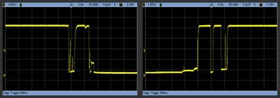
The big red button, being one of the most important components of our game, wasn’t simply plug and play. When you press the button, you expect it to only give one input to the microcontroller, but sometimes the microcontroller would instead receive two or more inputs. This is a common issue known as switch bouncing where the signal is very noisy (rapid changes in high and low logic levels) causing the microcontroller to think the button was pressed and released many times. Below are waveforms to help visualize the noise in action when a button is being pressed and released.
We have decided to fix this problem through hardware and debounce the button by implementing a simple RC circuit. Through the use of two resistors and a capacitor shown in the configuration below, we can filter out the noise and smooth the output of the switch signal going into the microcontroller.
Software Design
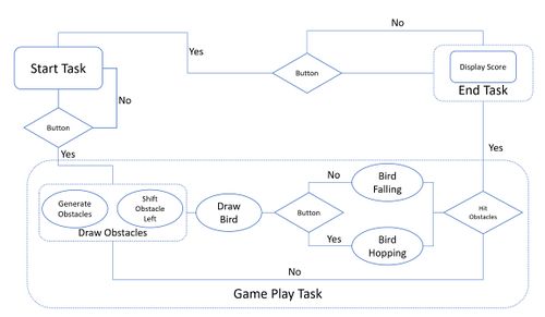
As there is only one input for the game. It must be differentiated which state the game is currently at. Below is the game logic.
There are three main stages on the software stack:
+ Start Task: Shifting the bird up-and-down and display the game title
+ Game Play Task: Draw birds, obstacles, and the basic gameplay of Flappy Bird
+ End Task: Display Score
During the start stage, when the button is pressed it will move on to the Game Play Task.
During the playing stage, when the button is pressed it will move the bird up 2 pixels and play the flying sound.
During the end stage, when the button is pressed it will return back to the start stage
Game Level:
For our implementation, we can increase the speed of the obstacles being generated. Pass 30 poles will result in the speed is increased by 1 level. Details on obstacles generation is below.
Obstacles Generations
Generating the obstacles onto the screen was a little tricky. The main algorithm is to first create one instance of an obstacle (one set of top and bottom poles) inside of an obstacle matrix (obs_matrix), then shifting one column at a time into an obstacle buffer (obsbuff), then finally copying that buffer over to the main led matrix buffer (matrixbuff). In order to create one instance of an obstacle inside obs_matrix, we make use of the structure (obs_hole_pos) that essentially contains two high and low coordinates (hi_pos and low_pos) of where to generate the hole (space between top and bottom poles). First, we fill the whole obs_matrix as if there is no hole, then use the hi_pos and low_pos values to generate the hole. For example, creating an obstacle with the high and low position of {5, 16} (hi_pos, low_pos) with an obstacle width of 4 looks like this:
Testing & Technical Challenges
Describe the challenges of your project. What advise would you give yourself or someone else if your project can be started from scratch again? Make a smooth transition to testing section and described what it took to test your project.
For our project we ran into many road block that were amplified due to the current state of affairs. Our advice would be to get the hardware layout done ASAP so PCB design and ordering can began. This will give some leeway for shipping delays, bad products, and debugging time.
Testing the project itself was not hard, but time was definitely an invaluable resource. Testing the parts individually (cables, PCB, LED matrix, etc) was simple but time consuming. To test our parts we utilized a multi-meter to check continuity on the PCB connections and our soldering work. A mistake we made was not testing our ribbon cables, which damaged one of our SJ2s when we switched out our GPIO cables.
Major Challenges:
1. Estimated Delivery of Parts
We faced some unexpected issues when gathering all the components for our project. Several parts came in late like our LED matrix and sometimes were dead-on-arrival. This issue was the worst regarding our PCB parts. Components such as the 2x20 headers and ribbon cable were delayed and did not arrive in a reasonable amount of time. Looking back, ordering the parts online was not ideal. Going to a parts store such as Anchor electronics would have saved us many of the headaches waiting for common parts to arrive.
2. Shoddy Quality Parts
Parts we ordered from amazon and parts from our local electronics shop proved to be faulty. Two LED matrixes did not properly light-up and it was not until our third matrix were we able to get a working one. The ribbon cables we used in our project were also shorted, which resulted in us shorting one of our SJ2s. To resolve this issue we should have budgeted extra time to individually check cable connections.
3. Music/Sound Effect Playback
One of the issues we experienced was our speakers only outputting noise during final project testing. This issue did not show up when testing parts individually using the SJ2 as a 3.3V power source. The issue was however determined to be the SJ2. Although it correctly flashed code and ran the LED matrix or DAC+AMP individually without issue, when combined the DAC was unable to output music. Using a different groupmate's SJ2 solved the issue completely. This issue was most likely tied to us using a faulty ribbon cable that only partially damaged our SJ2 board.
4. RGB LED Matrix Irregular Brightness
This is an issue we could not resolve in time before project submission. When our project was connection via GPIO pins it looked perfect. When connected through our PCB however, several rows of LEDs would shine brighter than the rest. Seeing this to be the case we determined the issue to most likely be noise at the PCB level.
Conclusion
Conclude your project here. You can recap your testing and problems. You should address the "so what" part here to indicate what you ultimately learnt from this project. How has this project increased your knowledge?
For our project we successfully created our game with our the designed game mechanics. The overall project however, was hindered by our poor time management. Many of the major problems encountered could have been solved more elegantly given more time and more rigorous testing. Overall, the biggest lesson we learned from the project is time & project management. Utilizing our time more wisely would have allowed us to allocate more resources into problem solving and additional gameplay features.
All in all, the project was a demonstration of the FreeRTOS knowledge learned in CMPE244 to create a deliverable.
Project Source Code
References
Acknowledgement
Any acknowledgement that you may wish to provide can be included here.
