Difference between revisions of "S17: Boom-Z Equalizer"
Proj user14 (talk | contribs) (→LED Matrix) |
Proj user14 (talk | contribs) (→LED Matrix) |
||
| Line 349: | Line 349: | ||
<span style="color:red">Put LED Matrix TESTING HERE </span> | <span style="color:red">Put LED Matrix TESTING HERE </span> | ||
| + | Testing testing | ||
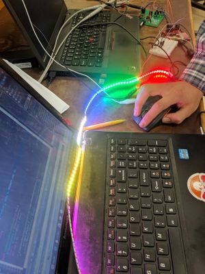
[[File:CmpE244 S17 TZFORCE LEDTest.jpg|left|thumb|300px|Test set up for the LED strips]] | [[File:CmpE244 S17 TZFORCE LEDTest.jpg|left|thumb|300px|Test set up for the LED strips]] | ||
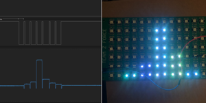
[[File:CmpE244 S17 TZFORCE 1kHzTest.png|right|thumb|300px|1kHz frequency test]] | [[File:CmpE244 S17 TZFORCE 1kHzTest.png|right|thumb|300px|1kHz frequency test]] | ||
| + | |||
| + | testing testing sdfsdf | ||
=== Technical Challenges === | === Technical Challenges === | ||
Revision as of 21:19, 25 May 2017
Contents
Grading Criteria
- How well is Software & Hardware Design described?
- How well can this report be used to reproduce this project?
- Code Quality
- Overall Report Quality:
- Software Block Diagrams
- Hardware Block Diagrams
- Schematic Quality
- Quality of technical challenges and solutions adopted.
Boom-Z Equalizer
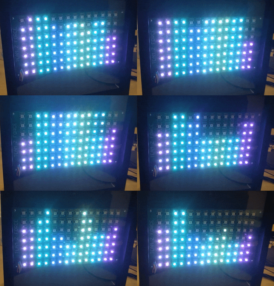
Abstract
The purpose of this project is to allow the team to experiment with a sound reactive project. The team will use a specialized IC to convert the input audio signal into a digital signal that can be parsed by the SJSUone board. The team will also create the LED array grid that will be used to display the waveform/frequency representation of the audio signal. The final project should be able to take an input audio signal (using a regular audio cable/jack) and display some kind of frequency representation using the LED array grid.
Objectives & Introduction
Show list of your objectives. This section includes the high level details of your project. You can write about the various sensors or peripherals you used to get your project completed.
Introduction
The team split the project into two parts: The equalizer and the LED Matrix part. Thus, the team split into two sub-teams to tackle these two parts separately. The Equalizer task focuses on the conversion of audio input into an ADC output that can be parsed and create a data representation for the LED Matrix task. The LED Matrix task's main focus is to parse the converted data and drive the LEDs to display the appropriate representation of the signals.
Objectives
Follow proper engineering and testing practices to design and implement the following:
- Design equalizer hardware
- Design equalizer PCB
- Design LED Matrix hardware
- Design overall software architecture
- Implement equalizer driver
- Implement LED matrix driver
- Integrate equalizer and LED matrix
- Test overall system
Team Members & Responsibilities
- David Bui
- Equalizer Hardware Design
- Equalizer PCB Design
- Marvin Flores
- Overall software design
- Equalizer driver
- Adam Iglesias
- LED Matrix driver
- Mina Yi
- LED Matrix hardware design
Schedule
| Week# | Date | Task | Actual |
|---|---|---|---|
| 1 | 3/19 |
|
|
| 2 | 3/26 |
|
|
| 3 | 4/2 |
|
|
| 4 | 4/9 |
|
|
| 5 | 4/16 |
|
|
| 6 | 4/23 |
|
|
| 7 | 4/30 |
|
|
| 8 | 5/7 |
|
|
| 9 | 5/14 |
|
|
| 10 | 5/21 |
|
|
Parts List & Cost
Bill of Materials for Graphic Equalizer
| # | Name | Purchase Location | Description | Quantity | Cost |
|---|---|---|---|---|---|
| 1 | MSGEQ7 | DigiKey | 7 Band Graphic Equalizer | 2 | $4.95 |
| 2 | capacitor | HSC Electronics | .1 uF capacitor | 7 | $0.35 |
| 3 | capacitor | HSC Electronics | 33 pF capacitor | 2 | $0.40 |
| 4 | capacitor | HSC Electronics | .33 uF capacitor | 1 | $0.35 |
| 5 | capacitor | HSC Electronics | 10 uF capacitor | 1 | $0.35 |
| 6 | capacitor | HSC Electronics | 100 nF capacitor | 1 | $0.35 |
| 7 | resistor | HSC Electronics | 200kΩ resistor | 2 | $0.05 |
| 8 | resistor | HSC Electronics | 22kΩ resistor | 2 | $0.05 |
| 9 | power jack | HSC Electronics | power jack | 1 | $0.45 |
| 10 | audio jack | HSC Electronics | audio jack | 1 | $0.45 |
| 11 | voltage regulator | HSC Electronics | 3V voltage regulator | 1 | $0.25 |
| 12 | voltage regulator | HSC Electronics | 5V voltage regulator | 1 | $0.25 |
| 13 | male header pins | HSC Electronics | male header pins | 1 | $0.95 |
Bill of Materials for LED Matrix
| # | Name | Purchase Location | Description | Quantity | Cost per item |
|---|---|---|---|---|---|
| 1 | LED Strip | Amazon | APA102C LEDs | 1 | $29.88 |
| 2 | PCB | Bay Area Circuits | 9.6" x 5" | 1 | $30 |
| 3 | Shadowbox | Michaels | 10" x 10", 4.5" depth | 1 | $32.99 |
| 4 | Thin Plywood | Home Depot | 9.5" x 9.5" | 1 | Varies |
| 5 | Power Supply | Amazon | Mean Well 5v 5A power supply | 1 | $13.22 |
| 6 | 3 Pronged Power Cord | Home Depot | Husky 8ft 3 pronged power replacement cord | 1 | $9.97 |
Design & Implementation
The design section can go over your hardware and software design. Organize this section using sub-sections that go over your design and implementation.
Hardware Design
Graphic Equalizer
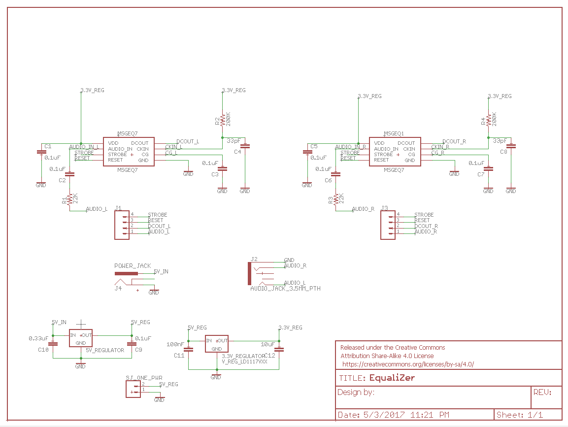
The main purpose of the graphic equalizer is to be able to take an audio input and generate an ADC output signal. The output values will be used to drive the LED Matrix values. The team decided to use MSGEQ7 chip for its simple design and ease of use. The MSGEQ7 Graphic equalizer can take an audio signal and 'split' it into 7 different frequencies. The team used two MSGEQ7 chips to separate left and right audio signal; this allowed the team to have more column of frequencies to display in the LED matrix.
The board design is very straight forward. The strobe and reset sources are driven at the same time to both MSGEQ7 chips; left and right audio input are split to each designated MSGEQ7 chip. The output for both chips are fed into the ADC inputs of the SJSUOne board. Voltage regulators are added to power the equalizer system and the SJSUOne board using one DC adapter. The tricky part was to write the software driver to parse the frequency outputs which will be discussed in the software implementation below.
Figure 1. Equalizer Schematic
LED Matrix
The LED matrix went through multiple changes throughout the project, but those will be discussed in the Testing & Technical Challenges section.
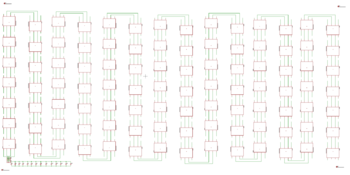
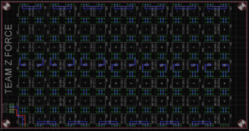
A PCB was designed to solder each LED via a plated through-hole. This was done because the LEDs come in a strip that needed to be cut to separate them. It was then possible to solder wires onto each of the copper pads to make the legs of the LED module.
Since the actual APA102C module was already soldered onto the LED strip, we had to create our own library module for the PCB board. To do this we:
- Created the symbol. The symbol is the image that is displayed on the schematic.
- Created the package which is the physical representation of the part. Also known as the footprint. This is also where you assign names to your pins.
- Created the device which combines the symbol and the package data.
Once our library was created, we began the PCB design. We opened the schematic alongside the board layout, to ensure that everything was updated at the same time, and added our LED module library to the schematic by choosing Library → Use.
From there, it was a matter of placing the modules onto the schematic and routing them on the board. We used the polygon tool to select the entire board to place one copper plane for our VCC and the same was done with ground. We were able to verify the routing via the Ratsnest tool.
Once the design was complete, we ran the DRC (design rule check) and ERC (electrical rule check) to ensure that our design was done properly. In addition to the default DRU, we used the OshPark DRU as an extra test.
The PCB was also verified by Bay Area Circuits when we placed the order. It took about a week for the board to be completed.
Overall, our PCB design consists of the following:
- 98 LEDs (7x14) that make up our matrix using our own library
- 2 Sets of header pins (connected) for VCC, data in, ground, and SCK
- This was added as an extra precaution since it is a high current drawing device, in case of pin damage
- 14 surface mount capacitors
- In case of signal stability (voltage drops) to help stabilize our design. We ended up not needing to add these.
- 4 through-holes on each corner for stand-offs
Hardware Interface
In this section, you can describe how your hardware communicates, such as which BUSes used. You can discuss your driver implementation here, such that the Software Design section is isolated to talk about high level workings rather than inner working of your project.
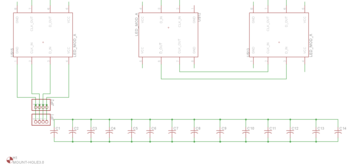
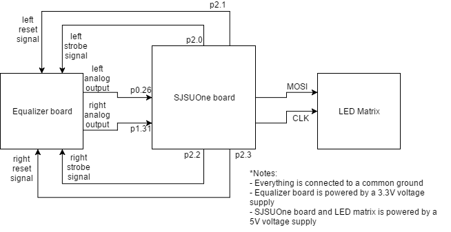
The Equalizer board is driven using 4 GPIO pins. Two pins are used for left and right strobe pins, while the other two are used for resetting each MSGEQ7 chips. 2 ADC pins are used to read the chips' analog outputs. SJSUOne board's SPI interface was used to drive the LED matrix.
Figure 2. Hardware interface
Software Design
Show your software design. For example, if you are designing an MP3 Player, show the tasks that you are using, and what they are doing at a high level. Do not show the details of the code. For example, do not show exact code, but you may show psuedocode and fragments of code. Keep in mind that you are showing DESIGN of your software, not the inner workings of it.
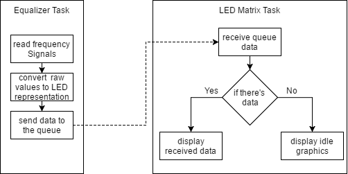
The Equalizer task reads analog values from the Equalizer Board and converts them into LED Matrix representation values. The analog input values are converted to digital using the onboard ADC. The converted values are then sent to the queue which the Matrix LED driver task is listening. The Matrix LED driver interprets the data and drives the LEDs to display the appropriate signal representation.
Figure 3. Software diagram
Implementation
This section includes implementation, but again, not the details, just the high level. For example, you can list the steps it takes to communicate over a sensor, or the steps needed to write a page of memory onto SPI Flash. You can include sub-sections for each of your component implementation.
Equalizer
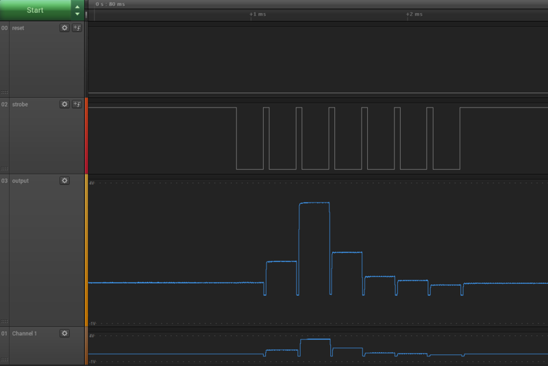
The MSGEQ7 chip has a unique way of outputting the analog signals (as shown in the strobe timing diagram below). The software needs to drive the GPIO pins to generate the strobe signal. The strobe signal is needed to be precisely controlled in order to read the analog outputs properly. Fortunately, the chip doesn't have a very strict timing and only has minimum values for signal widths.
Figure 4. Strobe Timing diagram
The code below shows the ADC reading implementation. As shown, the task loops for 7 times to read 7 different frequencies (for left and right outputs.) A struct was used to represent the frequency values and to make it easier to send to a queue. Take note that the reading only occurs when the strobe pins are driven low. In order to read the next frequency, the strobe pins need to be driven high and then low again.
Code snippet

for(int i = 0; i<7; i++) {
    clear_pin(STROBE_PIN_LEFT); //Clear Strobe_Pin 2.0
    clear_pin(STROBE_PIN_RIGHT); //Clear Strobe_Pin 2.2
    current_time_us = sys_get_uptime_us() + 36;
    while(sys_get_uptime_us() < current_time_us);

    uint16_t leftRawValue =  readPinValueP026();
    uint16_t rightRawValue = readPinValueP131();
    frequencyData.left[i] = convertSignalToMatrixReadable(leftRawValue);
    frequencyData.right[i] = convertSignalToMatrixReadable(rightRawValue);

    set_pin(STROBE_PIN_LEFT); //Set Strobe_Pin 2.0
    set_pin(STROBE_PIN_RIGHT); //Set Strobe_Pin 2.2
    current_time_us = sys_get_uptime_us() + 36;

    while(sys_get_uptime_us() < current_time_us);
}
After this loop, the frequencyData is sent to a queue. The LED Matrix tasks listen to this queue and process the received data to drive the LED Matrix display.
LED Matrix
To properly display on the LED matrix the received data from the equalizer the SPI communication bus must first be configured. The SPI protocol is what we used to send frequency data to LEDs. The SPI bus was configured to operate at 12mHz thus providing an ample refresh rate for the LED matrix. To send valid data to the LED, the Apa-102c is designed to intially recieving a 'start' over the MOSI line consisting of 32 bits of 0's.This is followed by a an N number of LED frames consisting of 3 bits of 1's ,followed by a 5 bit brightness setting and then 8 bits of blue,green and red values.
Testing & Technical Challenges
Describe the challenges of your project. What advise would you give yourself or someone else if your project can be started from scratch again? Make a smooth transition to testing section and described what it took to test your project.
Include sub-sections that list out a problem and solution, such as:
Testing
Equalizer
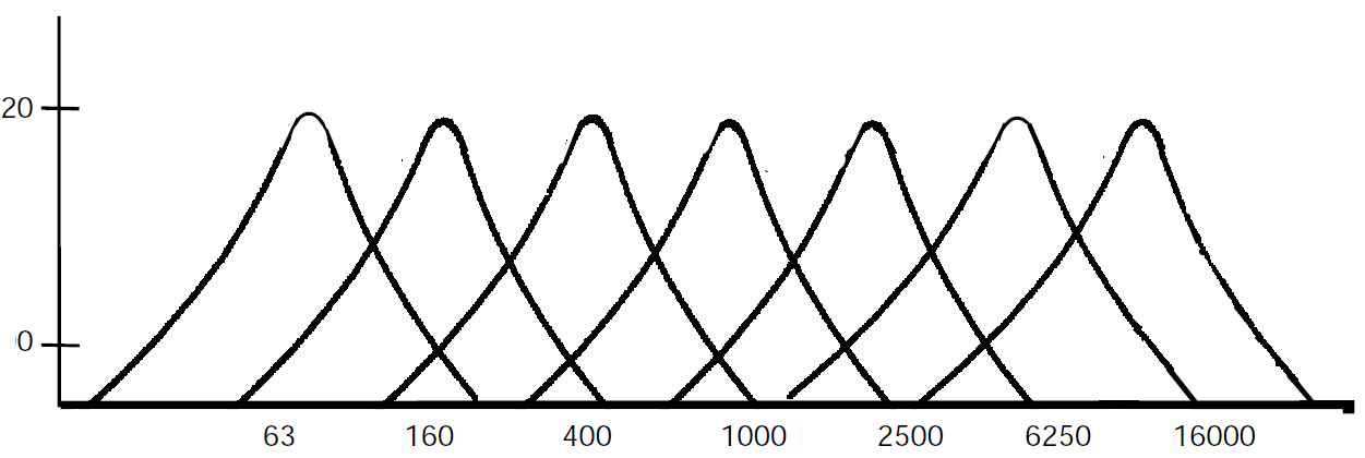
The team used Salaeae Logic Analyzer and an online frequency generator to test the equalizer. The output of the logic analyzer must match the MSGEQ7's frequency response. Notice that the output would not give a perfect filtered value but a half-waveform that peaks at the target frequency.
LED Matrix
Put LED Matrix TESTING HERE
Testing testing
testing testing sdfsdf
Technical Challenges
Equalizer Design
- Generating strobe and reading the ADC values need precise timing. One missed reading will messed up the data representation of the frequency values.
- Using digital analyzer greatly helped the team debug the timing issues.
- The MSGEQ7 chip is very sensitive to noise. In reality, this chip wouldn't perfectly filter-out the surrounding frequencies; thus we should look only to whether or not the target frequency has the highest output voltage.
- Using online frequency generators, together with the logic analyzer, helped the team debug the system.
LED Matrix Design
- Not all LEDs are created equal. The first set of LEDs that we bought used a non-standard communication protocol with very precise timing (in nanoseconds)
- The team decided to move on and use a different kind of LEDs which use a standard SPI protocol
- Soldering LEDs is very time consuming and prone to mistakes.
- Since we can't solder them earlier as expected, the team decided to create a back-up LED matrix board just in case the main LED matrix doesn't work.
Discuss the issue and resolution.
Conclusion
Conclude your project here. You can recap your testing and problems. You should address the "so what" part here to indicate what you ultimately learnt from this project. How has this project increased your knowledge?
Project Video
Upload a video of your project and post the link here.
Project Source Code
References
Acknowledgement
Any acknowledgement that you may wish to provide can be included here.
References Used
List any references used in project.
Appendix
You can list the references you used.
