Difference between revisions of "S14: Hyperintelligent NFC Locker of the Future"
Proj user8 (talk | contribs) (→Hardware Design) |
Proj user8 (talk | contribs) (→Design & Implementation) |
||
| Line 174: | Line 174: | ||
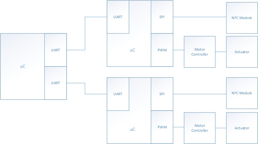
As shown above, the NFC locker system is composed of three uC: Two masters and one shared slave. The two masters drive their independent actuator subsystem, independent NFC module subsystem, and shares the slave. | As shown above, the NFC locker system is composed of three uC: Two masters and one shared slave. The two masters drive their independent actuator subsystem, independent NFC module subsystem, and shares the slave. | ||
| + | |||
The masters pull data from its NFC subsystem, and sends the data to the slave. The slave will either accept or reject the password. If the password is verified, the slave will then send information to the master, where the actuator subsystem will either lock or unlock the locker. | The masters pull data from its NFC subsystem, and sends the data to the slave. The slave will either accept or reject the password. If the password is verified, the slave will then send information to the master, where the actuator subsystem will either lock or unlock the locker. | ||
| + | ===Power System Design=== | ||
[[File:CmpE146 S14 NFCLocker PowerDiagram.jpg]] | [[File:CmpE146 S14 NFCLocker PowerDiagram.jpg]] | ||
| + | |||
| + | |||
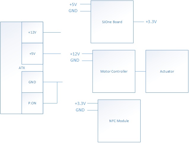
| + | The system ranges in using three different voltages: +12V, +5V, and +3.3V. Because these voltages are standard in computer systems, the team used an ATX power supply. The ATX power supply has a +12V, +5V, and a +3.3V output. | ||
| + | |||
| + | Actuator Subsystem: | ||
| + | The motor controllers which drives the actuators needs at least a +12V supply, because it requires a heavy amount of current to drive the actuator. | ||
| + | |||
| + | Micro-controllers: | ||
| + | The SJOne Boards can be powered with a +5V supply. The team used the ATX's +5V output to power each uC. | ||
| + | |||
| + | NFC Subsystem: | ||
| + | The NFC module can be powered with either a +5V or +3.3V supply. For convenience, the team used the uC's 3.3V output to drive the NFC module. | ||
| + | |||
====Locker System Design==== | ====Locker System Design==== | ||
Revision as of 18:53, 20 May 2014
Contents
- 1 Grading Criteria
- 2 Hyperintelligent NFC Locker of the Future
- 3 Abstract
- 4 Objectives & Introduction
- 5 Schedule
- 6 Parts List & Cost
- 7 Design & Implementation
- 8 Testing & Technical Challenges
- 9 Conclusion
- 10 References
Grading Criteria
- How well is Software & Hardware Design described?
- How well can this report be used to reproduce this project?
- Code Quality
- Overall Report Quality:
- Software Block Diagrams
- Hardware Block Diagrams
- Schematic Quality
- Quality of technical challenges and solutions adopted.
Hyperintelligent NFC Locker of the Future
Abstract
This section should be a couple lines to describe what your project does.
The team's idea behind the Hyperintelligent NFC Locker of the Future was to reinvent the currently outdated system of rental lockers. Current rental lockers require a user to input money to release a key and lock the locker. Then, when the user is done with the locker, they use the key to unlock the locker and the key is now stuck there for the next user. The Hyperintelligent NFC Locker of the Future is modernizing this process by using NFC technology from a user's smartphone as the "key".
Objectives & Introduction
Show list of your objectives. This section includes the high level details of your project. You can write about the various sensors or peripherals you used to get your project completed.
Objectives
The objectives of the Hyperintelligent NFC Locker of the Future include:
Introduction
A user of the Hyperintelligent NFC Locker of the Future will walk up to a locker not being used and request a key by placing his/her phone on the NFC module. The key will save to the phone application. After receiving the key, the user can now lock the locker by issuing a lock command with the phone application and saved key. After unlocking the locker, the key will now be erased so the user can't use the lock again unless they go through the process again.
Team Members & Responsibilities
- Devin Villarosa
- Driver Development, Project Manager
- Hien Nguyen
- Locker Construction, Mobile Application Development
- Gregory Pace
- FreeRTOS Software Design, Networking
Schedule
Show a simple table or figures that show your scheduled as planned before you started working on the project. Then in another table column, write down the actual schedule so that readers can see the planned vs. actual goals. The point of the schedule is for readers to assess how to pace themselves if they are doing a similar project.
| Week# | Task | Projected Completion Date | Actual Completion Date | Status | Notes |
|---|---|---|---|---|---|
| 1 | Order Parts | 3/21 | 3/21 | Completed | Some changes to the designs were made and extra parts were ordered after the initial date. |
| 2 | NFC Module | 3/28 | Incomplete | Documentation was limited and getting started on the code was difficult | |
| 3 | Locker Application | 4/4 | 4/18 | Completed | Constructing the locker was fairly quick and simple. However, figuring out how to attach our locking mechanism and place our components in the box took longer than expected. |
| 4 | Android Smartphone Application | 4/11 | Incomplete | A lot of documentation on NFC applications is provided by Android. | |
| 5 | Communication Between Phone and Locker | 4/18 | Incomplete | ||
| 6 | Implementing a Two Locker System | 4/25 | Incomplete | Actual completion date was pushed back to do difficulties of finishing the NFC module component. | |
| 7 | Reserved to Catch Up | 5/2 | Incomplete | Used time to figure out how to get NFC module to work. | |
| 8 | Reserved to Catch Up | 5/9 | Incomplete | Finalized NFC module and multiple locker system. | |
| 9 | Final Tests and Aesthetics | 5/16 | Incomplete |
Parts List & Cost
Give a simple list of the cost of your project broken down by components. Do not write long stories here.
| Quantity | Part | Price Per Unit | |
|---|---|---|---|
| 1 | (3) | SJ One Board | $80 |
| 2 | (1) | 1 in. x 12 in. x 8 ft. Select Pine Board | $33.46 |
| 3 | (2) | ITEAD PN532 NFC MODULE | $17.00 |
| 4 | (2) | Universal Heavy Duty Power Door Lock Actuator Motor 2 Wire 12V | $5.13 |
| 5 | (2) | Leegoal L298N Stepper Motor Driver Controller Board Module | $7.50 |
| 6 | (2) | ENC28J60 Ethernet LAN Network Module For 51 AVR STM32 LPC | $7.31 |
| 7 | (1) | TRENDnet 5-Port Unmanaged 10/100 Mbps GREENnet Ethernet Desktop Plastic Housing Switch, TE100-S5 | $9.99 |
| 8 | (1) | Logisys 480W 240-Pin Dual Fan 20+4 ATX Power Supply PS480D2 | $13.99 |
Design & Implementation
The design section can go over your hardware and software design. Organize this section using sub-sections that go over your design and implementation.
Hardware Design
As shown above, the NFC locker system is composed of three uC: Two masters and one shared slave. The two masters drive their independent actuator subsystem, independent NFC module subsystem, and shares the slave.
The masters pull data from its NFC subsystem, and sends the data to the slave. The slave will either accept or reject the password. If the password is verified, the slave will then send information to the master, where the actuator subsystem will either lock or unlock the locker.
Power System Design
The system ranges in using three different voltages: +12V, +5V, and +3.3V. Because these voltages are standard in computer systems, the team used an ATX power supply. The ATX power supply has a +12V, +5V, and a +3.3V output.
Actuator Subsystem: The motor controllers which drives the actuators needs at least a +12V supply, because it requires a heavy amount of current to drive the actuator.
Micro-controllers: The SJOne Boards can be powered with a +5V supply. The team used the ATX's +5V output to power each uC.
NFC Subsystem: The NFC module can be powered with either a +5V or +3.3V supply. For convenience, the team used the uC's 3.3V output to drive the NFC module.
Locker System Design
Hardware Interface
In this section, you can describe how your hardware communicates, such as which BUSes used. You can discuss your driver implementation here, such that the Software Design section is isolated to talk about high level workings rather than inner working of your project.
Power Hardware Interface
Locker System Interface
Software Design
Show your software design. For example, if you are designing an MP3 Player, show the tasks that you are using, and what they are doing at a high level. Do not show the details of the code. For example, do not show exact code, but you may show psuedocode and fragments of code. Keep in mind that you are showing DESIGN of your software, not the inner workings of it.
BLAHBLAHB:AH
asdfsadfs
NFC Software Design
Phone Application Software Design
UART Communication Software Design
Actuator Software Design
Implementation
This section includes implementation, but again, not the details, just the high level. For example, you can list the steps it takes to communicate over a sensor, or the steps needed to write a page of memory onto SPI Flash. You can include sub-sections for each of your component implementation.
NFC Software Implementation
Phone Application Software Implementation
UART Communication Software Implementation
Actuator Software Implementation
Testing & Technical Challenges
Describe the challenges of your project. What advise would you give yourself or someone else if your project can be started from scratch again? Make a smooth transition to testing section and described what it took to test your project.
Include sub-sections that list out a problem and solution, such as:
My Issue #1
Discuss the issue and resolution.
Conclusion
Conclude your project here. You can recap your testing and problems. You should address the "so what" part here to indicate what you ultimately learnt from this project. How has this project increased your knowledge?
Project Video
Upload a video of your project and post the link here.
Project Source Code
Send me your zipped source code and I will upload this to SourceForge and link it for you.
References
Acknowledgement
Any acknowledgement that you may wish to provide can be included here.
We would like to acknowledge Preetpal Kang and Dr. Haluk Özemek for giving us strength.
References Used
List any references used in project.


