Difference between revisions of "F13: Vehicle On Board Diagnostics"
Proj user11 (talk | contribs) (→Design & Implementation) |
(→Project Video) |
||
| (11 intermediate revisions by 2 users not shown) | |||
| Line 1: | Line 1: | ||
| − | |||
| − | |||
| − | |||
| − | |||
| − | |||
| − | |||
| − | |||
| − | |||
| − | |||
| − | |||
| − | |||
| − | |||
== Vehicle On Board Diagnostics == | == Vehicle On Board Diagnostics == | ||
| Line 19: | Line 7: | ||
== Objectives & Introduction == | == Objectives & Introduction == | ||
| − | *Extract RPM | + | *Extract RPM and Speed data from vehicle |
*Interface with vehicle through UART bus by means of the On Board Diagnostic OBDII connector | *Interface with vehicle through UART bus by means of the On Board Diagnostic OBDII connector | ||
*Data sent to LCD and displayed to user using either UART, I2C, or SPI bus | *Data sent to LCD and displayed to user using either UART, I2C, or SPI bus | ||
| Line 61: | Line 49: | ||
| 11/4 | | 11/4 | ||
| SPI interface with LCD display, Setup SPI H/W | | SPI interface with LCD display, Setup SPI H/W | ||
| − | | | + | | N |
|- | |- | ||
! scope="row"| 6 | ! scope="row"| 6 | ||
| 11/11 | | 11/11 | ||
| SPI to SD card interface | | SPI to SD card interface | ||
| − | | | + | | Y |
|- | |- | ||
! scope="row"| 7 | ! scope="row"| 7 | ||
| 11/18 | | 11/18 | ||
| Purchase enclosure, Perform integration and test | | Purchase enclosure, Perform integration and test | ||
| − | | | + | | Y |
|- | |- | ||
! scope="row"| 8 | ! scope="row"| 8 | ||
| 11/25 | | 11/25 | ||
| Debug and Complete wikipedia report | | Debug and Complete wikipedia report | ||
| − | | | + | | Y |
|- | |- | ||
! scope="row"| 9 | ! scope="row"| 9 | ||
| 12/2 | | 12/2 | ||
| Prepare Presentation | | Prepare Presentation | ||
| − | | | + | | Y |
|- | |- | ||
|} | |} | ||
| Line 106: | Line 94: | ||
|- | |- | ||
! scope="row"| 3 | ! scope="row"| 3 | ||
| − | | | + | | Cell Phone Battery Charger |
| − | | | + | | 1 |
| − | | | + | | 20.95 |
| + | |- | ||
|- | |- | ||
! scope="row"| 4 | ! scope="row"| 4 | ||
| − | |||
| − | |||
| − | |||
| − | |||
| − | |||
| Micro SD Card 2 GB | | Micro SD Card 2 GB | ||
| 1 | | 1 | ||
| 5.00 | | 5.00 | ||
|- | |- | ||
| − | ! scope="row"| | + | ! scope="row"| 5 |
| LCD Display, NHD-0420D3Z-NSW-BBW-V3 | | LCD Display, NHD-0420D3Z-NSW-BBW-V3 | ||
| 1 | | 1 | ||
| 25.90 | | 25.90 | ||
|- | |- | ||
| − | ! scope="row"| | + | ! scope="row"| 6 |
| SJ One Board | | SJ One Board | ||
| 1 | | 1 | ||
| 75.00 | | 75.00 | ||
|- | |- | ||
| − | ! scope="row"| | + | ! scope="row"| 7 |
| Total | | Total | ||
| | | | ||
| − | | | + | | 196.80 |
|- | |- | ||
|} | |} | ||
| Line 165: | Line 149: | ||
=== Hardware Interface === | === Hardware Interface === | ||
| − | + | UART Bus | |
| + | *UART 2 connection between the SJ One Board to the OBDII to UART board through Rx and Tx communication lines | ||
| + | *SJ One Board pins P0.10 "TXD2" and P0.11 "RXD2" interface to OBDII to UART board's RX-1 and TX-0 through jumper wires | ||
| + | |||
| + | SPI Bus | ||
| + | *SPI connection with onboard micro SD card and LCD display | ||
| + | *Place micro SD card in micro SD card holder | ||
| + | *Utilized SPI 1 connection between the SJ One Board and the LCD display from New Haven | ||
| + | *SJ One Board pins P0.9 "MOSI1", P0.7 "SCK1", and P1.28 "GPIO" connected to New Haven LCD Display J2 pin4 "SPI Data", J2 pin3 "SPI CLK", and J2 pin1 "SPI Slave Select" | ||
| + | |||
| + | I2C Bus (did not function) | ||
| + | *Alternative, I2C 2 connection between the SJ One Board and the LCD Display | ||
| + | *SJ One Board pins P0.10 "SDA2" and P0.11 "SCL2" to LCD Display J2 pin4 "I2C data" and J2 pin4 "I2C clock" | ||
| + | *Observe that the pins interfere with the UART 2 connection so adaptation to a different UART port is necessary | ||
| + | |||
| + | Power and Grounding | ||
| + | *5V/1A Power is derived from the battery USB interface, a spliced USB cord directs power to the LCD and the SJ One Board | ||
| + | *The battery is rechargeable for continued use | ||
| + | *Grounds from the SJ One Board, LCD, and OBDII to UART board are shorted together through on the SJ One board | ||
=== Software Design === | === Software Design === | ||
| − | The software | + | The software loops through a routine to retrieve information from the car's engine control unit (ECU). The routine is as follows. |
| − | + | *Send a 1 byte UART 2 command in hex | |
| − | + | *Read UART 2 output data | |
| + | *Process UART 2 data | ||
| + | *Send results to LCD through I2C or SPI | ||
| + | *Record results on micro SD card | ||
=== Implementation === | === Implementation === | ||
| Line 201: | Line 206: | ||
=== Project Video === | === Project Video === | ||
| − | + | * [http://youtu.be/MdjbbQKWd3E Project Video] | |
=== Project Source Code === | === Project Source Code === | ||
| − | + | * [https://sourceforge.net/projects/sjsu/files/CmpE240_LM_F2013/ Sourceforge link for source code] | |
== References == | == References == | ||
Latest revision as of 03:00, 8 December 2013
Contents
Vehicle On Board Diagnostics
Abstract
The goal of this project is to develop a monitoring system for an automobile utilizing the SJSU development board containing an ARM LPC1758 chip. The monitoring system shall obtain key parameters from the ECU of the vehicle, in this case a Honda Civic '05. These parameters shall be processed by the LPC1758 chip and distributed to the LCD screen and stored into the micro SD card. If time permitting, the monitoring system shall incorporate an interface to an mobile app.
This platform will provide a means of tracking car performance characteristics.
Objectives & Introduction
- Extract RPM and Speed data from vehicle
- Interface with vehicle through UART bus by means of the On Board Diagnostic OBDII connector
- Data sent to LCD and displayed to user using either UART, I2C, or SPI bus
- Data stored into micro SD card through SPI bus in a view able format for future processing on a PC.
Team Members & Responsibilities
- Jonathan
- Hardware and Software Designer
Schedule
Show a simple table or figures that show your scheduled as planned before you started working on the project. Then in another table column, write down the actual schedule so that readers can see the planned vs. actual goals. The point of the schedule is for readers to assess how to pace themselves if they are doing a similar project.
| Week# | Date | Task | Completed |
|---|---|---|---|
| 1 | 10/7 | Project Proposal | Y |
| 2 | 10/14 | Order Parts for Project | Y |
| 3 | 10/21 | Receive Parts and work on schedule | Y |
| 4 | 10/28 | UART to OBII communication, Setup UART H/W | Y |
| 5 | 11/4 | SPI interface with LCD display, Setup SPI H/W | N |
| 6 | 11/11 | SPI to SD card interface | Y |
| 7 | 11/18 | Purchase enclosure, Perform integration and test | Y |
| 8 | 11/25 | Debug and Complete wikipedia report | Y |
| 9 | 12/2 | Prepare Presentation | Y |
Parts List & Cost
Give a simple list of the cost of your project broken down by components. Do not write long stories here.
| Number | Description | Quantity | Price ($) |
|---|---|---|---|
| 1 | Car Diagnostic Kit, RTL-10769 | 1 | 59.95 |
| 2 | Male/Female Jumper Wires | 10 | 10.00 |
| 3 | Cell Phone Battery Charger | 1 | 20.95 |
| 4 | Micro SD Card 2 GB | 1 | 5.00 |
| 5 | LCD Display, NHD-0420D3Z-NSW-BBW-V3 | 1 | 25.90 |
| 6 | SJ One Board | 1 | 75.00 |
| 7 | Total | 196.80 |
Design & Implementation
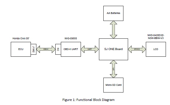
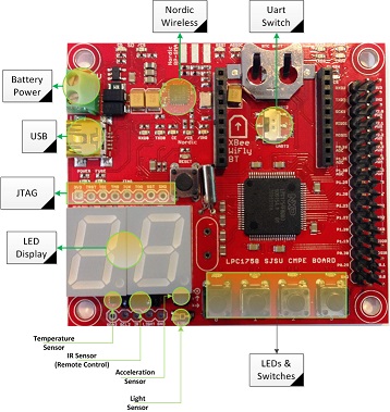
The hardware design focuses on the SJ One board. This board communicates to the peripheral devices through UART, SPI, and I2C bus interfaces while powered by AA batteries. The three peripheral devices are a Honda Civic engine control unit (ECU), a LCD, and a micro SD card. Between the ECU and SJ One board is an intermediate board that translates UART commands into OBDII commands.
The software design emphasizes a polling methodology. A large loop initiated by the user constantly requests information from the ECU through UART drivers. The returned data is in ASCII and converted into integers for processing. Once processed, the information is sent to the LCD for display and micro SD for storage through the SPI interface. This cycle is repeated until a memory limit or user stops the process.
Below is the overall functional block diagram.
Hardware Design
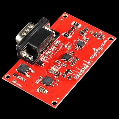
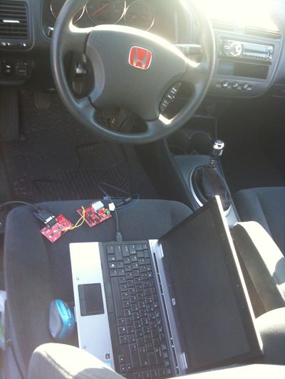
The hardware design's center is the SJ One board. There are three communication interfaces and one power interface. The first communication interface, UART2, utilizes pins TXD2 and RXD2 on the SJ One board. A jumper wire from TXD2 goes to the RX-1 pin and RXD2 goes to the TX-0 pin of the UART-OBDII board. Finally, a ground jumper between the boards completes the UART interface. From the UART-OBDII board, an RS232 to OBDII cable completes the connection to the car's ECU.
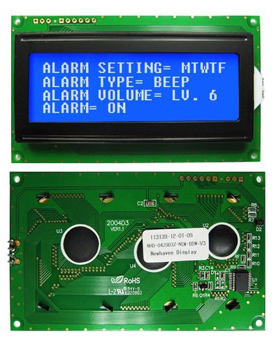
The second communication interface, SPI, bus, utilizes pins SCK1, MISO1, and MOSI1 to connect to the LCD's corresponding pins. To power the LCD, two jumpers are applied, one for the 5V input and one for the ground to the LCD display.
The last communication interface is already hardwired on the SJ One board. A micro SD card slot holder is available on the back of the board. You only need to install the card.
Discuss your hardware design here. Show detailed schematics, and the interface here.
Hardware Interface
UART Bus
- UART 2 connection between the SJ One Board to the OBDII to UART board through Rx and Tx communication lines
- SJ One Board pins P0.10 "TXD2" and P0.11 "RXD2" interface to OBDII to UART board's RX-1 and TX-0 through jumper wires
SPI Bus
- SPI connection with onboard micro SD card and LCD display
- Place micro SD card in micro SD card holder
- Utilized SPI 1 connection between the SJ One Board and the LCD display from New Haven
- SJ One Board pins P0.9 "MOSI1", P0.7 "SCK1", and P1.28 "GPIO" connected to New Haven LCD Display J2 pin4 "SPI Data", J2 pin3 "SPI CLK", and J2 pin1 "SPI Slave Select"
I2C Bus (did not function)
- Alternative, I2C 2 connection between the SJ One Board and the LCD Display
- SJ One Board pins P0.10 "SDA2" and P0.11 "SCL2" to LCD Display J2 pin4 "I2C data" and J2 pin4 "I2C clock"
- Observe that the pins interfere with the UART 2 connection so adaptation to a different UART port is necessary
Power and Grounding
- 5V/1A Power is derived from the battery USB interface, a spliced USB cord directs power to the LCD and the SJ One Board
- The battery is rechargeable for continued use
- Grounds from the SJ One Board, LCD, and OBDII to UART board are shorted together through on the SJ One board
Software Design
The software loops through a routine to retrieve information from the car's engine control unit (ECU). The routine is as follows.
- Send a 1 byte UART 2 command in hex
- Read UART 2 output data
- Process UART 2 data
- Send results to LCD through I2C or SPI
- Record results on micro SD card
Implementation
This section includes implementation, but again, not the details, just the high level. For example, you can list the steps it takes to communicate over a sensor, or the steps needed to write a page of memory onto SPI Flash. You can include sub-sections for each of your component implementation.
Testing & Technical Challenges
Describe the challenges of your project. What advise would you give yourself or someone else if your project can be started from scratch again? Make a smooth transition to testing section and described what it took to test your project.
Test Phase 1 UART to OBDII communication Test
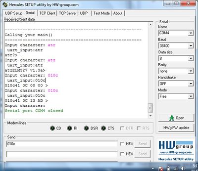
- Send individual commands to the car's ECU and receive RPM, temperature, and speed back
Include sub-sections that list out a problem and solution, such as:
My Issue #1
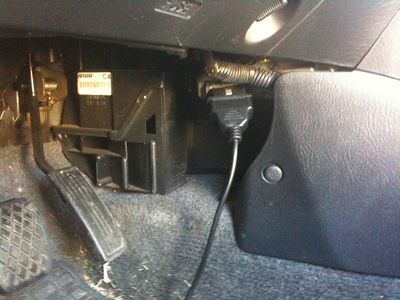
Initial Problem with UART to OBDII communication. The commands that were sent did not receive response. I noticed that the LEDs on the UART to OBDII board were flashing when they should not. I realized that I did not ground the board.
Conclusion
Conclude your project here. You can recap your testing and problems. You should address the "so what" part here to indicate what you ultimately learnt from this project. How has this project increased your knowledge?
Project Video
Project Source Code
References
Acknowledgement
Any acknowledgement that you may wish to provide can be included here.
References Used
List any references used in project.
Appendix
You can list the references you used.
