Difference between revisions of "S17: Smart Health Gear"
Proj user5 (talk | contribs) (→LCD) |
Proj user5 (talk | contribs) (→Abstract) |
||
| Line 15: | Line 15: | ||
== Abstract == | == Abstract == | ||
| − | In today's fast paced Environment, more and more people are taking benefits of the latest technologies to keep track of their own fitness level and health. Smart Health Gear is one such wearable device which will help in monitoring various aspects of a person's health like heart rate, body oxygen level, | + | In today's fast paced Environment, more and more people are taking benefits of the latest technologies to keep track of their own fitness level and health. This helps them to make wise health decisions or take immediate action to improve their health. Smart Health Gear is one such wearable device which will help in monitoring various aspects of a person's health like heart rate, body oxygen level, footsteps count and body temperature. It will come with a compatible Bluetooth based Android application which will notify the user on completion of daily activities and log all the data from the Smart Health Gear to provide a history chart. |
== Objectives & Introduction == | == Objectives & Introduction == | ||
Revision as of 12:55, 25 May 2017
Contents
- 1 Grading Criteria
- 2 Project Title
- 3 Abstract
- 4 Objectives & Introduction
- 5 Schedule
- 6 Parts List & Cost
- 7 Design & Implementation
- 8 Heart rate calculation
- 9 Android Application
- 10 Testing & Technical Challenges
- 11 Conclusion
- 12 References
Grading Criteria
- How well is Software & Hardware Design described?
- How well can this report be used to reproduce this project?
- Code Quality
- Overall Report Quality:
- Software Block Diagrams
- Hardware Block Diagrams
- Schematic Quality
- Quality of technical challenges and solutions adopted.
Project Title
Smart Health Gear
Abstract
In today's fast paced Environment, more and more people are taking benefits of the latest technologies to keep track of their own fitness level and health. This helps them to make wise health decisions or take immediate action to improve their health. Smart Health Gear is one such wearable device which will help in monitoring various aspects of a person's health like heart rate, body oxygen level, footsteps count and body temperature. It will come with a compatible Bluetooth based Android application which will notify the user on completion of daily activities and log all the data from the Smart Health Gear to provide a history chart.
Objectives & Introduction
Show list of your objectives. This section includes the high level details of your project. You can write about the various sensors or peripherals you used to get your project completed.
The objectives are as follows:
- To be able to calculate and continuously monitor the heart rate
- To be able to calculate the oxygen level in blood
- To be able to calculate the body temperature
- To be able to calculate the step count of the person
- To be able to view all the vital details on a wearable device having LCD
- To be able to view the same details on an Android app
Team Members & Responsibilities
- Aniket Dali
- Jean Mary
- Manoj Ramesh Rao
- Neha Biradar
- Sushma Macha
Schedule
Show a simple table or figures that show your scheduled as planned before you started working on the project. Then in another table column, write down the actual schedule so that readers can see the planned vs. actual goals. The point of the schedule is for readers to assess how to pace themselves if they are doing a similar project.
| Week# | Date | Task | Comments |
|---|---|---|---|
| 1 | 3/2 | Submission of Project Proposals | Completed |
| 2 | 3/15 | Gathering requirements | Completed |
| 3 | 3/30 | Finalizing and documenting project requirements | Completed |
| 4 | 4/5 | Initiate research on components and start research/development on algorithms to read sensor values. | Completed |
| 5 | 4/8 | Initiate development of sensor and IO modules in software. | Completed |
| 6 | 4/16 | Finish component procurement and start PCB design. Start research on strategies for unit and integration testing. | Completed |
| 7 | 4/18 | Designing code architecture and interfaces. Prepare test plan to unit test sensor and IO modules. | Completed |
| 8 | 4/23 | Finish unit test plan. Finish PCB design and Place and order for PCB fabrication . | Completed |
| 9 | 4/24 | Finish and document code architecture and initialize interfaces provided to RTOS application. Initiate designing of Android application. | Completed |
| 10 | 4/25 | Development of RTOS application to control sensor and IO modules. | Completed |
| 11 | 4/27 | Unit testing of sensor and IO modules and updating results. Initiate preparation of integration test plan. | Completed |
| 12 | 4/30 | Bug fixing and re-testing. Initiate Unit testing of RTOS application. | Completed |
| 13 | 5/2 | Bug fixing and re-testing for unit test phase. | Completed |
| 14 | 5/4 | Integration testing of sensor modules and RTOS application and update results. | Completed |
| 15 | 5/8 | Bug fixing and re-testing. Initiate PCB testing. | Completed |
| 16 | 5/12 | Bugs fixing and re-testing for integration and PCB. | Completed |
| 17 | 5/14 | Start System testing. | Completed |
| 18 | 5/16 | Bug fixing and re-testing.Initiate documentation of project report. | Completed |
| 19 | 5/19 | Bug fixing and re-testing.Finish project documentation. | Completed |
| 20 | 5/20 | Prepare release note. Ready for demo. | Completed |
| 22 | 5/23 | Demo. |
Parts List & Cost
| Item# | Part | Manufacturer | Part number | Cost($) |
|---|---|---|---|---|
| 1 | SJ One Board | Preet | n/a | 80.00 |
| 2 | Heart-Rate Monitor and Pulse Oximeter Sensor | Maxim | MAXREFDES117 | 20.00 |
| 3 | HC-06 wireless bluetooth transceiver | Banggood | Datasheet | 6.55 |
| 4 | 10K Precision Epoxy Thermistor - 3950 NTC | Adafruit | Lookup Table | 4.00 |
| 5 | LCD module | Aliexpress | SEN-10988 | 32.30 |
| 6 | Hardware | Excess Solution | Berg strips, Jumper wires, Connectors, Standoffs | 5.00 |
| 7 | 9V Battery | Amazon | 32.30 |
- Total Cost: 153.79$
Design & Implementation
The design section can go over your hardware and software design. Organize this section using sub-sections that go over your design and implementation.
Printed Circuit Board
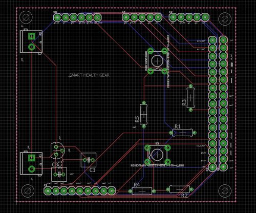
The PCB design was one of the challenging part of this project. The PCB design was created in Autodesk Eagle v8.1.0. Before proceeding with the schematic, we had decided to design a PCB that matches with the size of the SJ one board such that it could be mounted over it. Considering designing a wearable device, we had to keep in mind the form factor of the PCB. Initially we designed a PCB which turned out to be four-layer PCB including the blood pressure monitoring subsystem. However due to budget constraints we had to give up the blood pressure system as printing the same required a licensed version of Eagle.
Before starting the PCB schematic design, we decided on the location of sensors as it was vital for a wearable health monitoring device with a LCD display facing the user. Since surface mount soldering was not an option we decided to design the schematic with through hole connections. Another challenging part for our design was the libraries needed for schematic design. Since we didn’t have libraries for heart rate sensors, we had to design by creating it from scratch. However, we had some libraries from sparkfun, Eagle and Adafruit, the entire process took most of our time.
The first step in PCB design is to import all the libraries of the components that we would be using and create a schematic using the same. We made use of the Dimension tool in Eagle to match the PCB size with that of the SJ one board. We created the schematic by placing the required components and wiring them. The tutorial on Sparkfun website was very helpful in designing the same. It was very important for to ensure that all connections are verified properly before it gets printed. This was done using “DRC” Design Rule Check in Eagle which would show if any consistent errors existed.
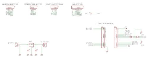
EAGLE Schematic
EAGLE Connector List
| Section | Connector | Library | Package | Device |
|---|---|---|---|---|
| Power Connector | 2x2-pin | SparkFun-Connectors | SCREWTERMINAL-3.5MM-2 | CONN_023.5MM (CONN_02) |
| SJ-One Board | 2x17-pin | SparkFun-Connectors | 1X17 | CONN_17 |
| Bluetooth Module | 1x6-pin | SparkFun-Connectors | 1X06 | CONN_06SILK_FEMALE_PTH (CONN_06) |
| Temperature Sensor | 1x5-pin | SparkFun-Connectors | 1X05 | CONN_05 |
| Heart Rate Sensor | 1x5-pin | SparkFun-Connectors | 1X05 | CONN_05 |
| LCD Section | 1x9-pin | SparkFun-Connectors | 1X09 | CONN_09 |
| Resistor | 5x2-pin | resistor | 0207/7 | R-US_0207/7 (R-US_) |
| Capacitor | 2x2-pin | rcl | C025-050X050 | C-US025-050X050 (C-US) |
| Switch | 2x4-pin | SparkFun-Switches | TACTILE_SWITCH_PTH_6.0MM | MOMENTARY-SWITCH-SPST-PTH-6.0MM (MOMENTARY-SWITCH-SPST) |
| LM7805 Regulator IC | 1x3-pin | v-reg | 78LXX | 78LXX |
Once the schematic is created that can be easily converted to Board Layout using the Generate/Switch to board option in Eagle. But this would create the board by randomly placing the parts at different locations. Since we had to have an LCD mount over the PCB as well as match the 17x2 connectors with that of SJ one board we created the design accordingly. After ensuring that everything was in place we placed order for the PCB and verified the same again using a multi-meter if all the connections were correct.
Hardware Design
Discuss your hardware design here. Show detailed schematics, and the interface here.
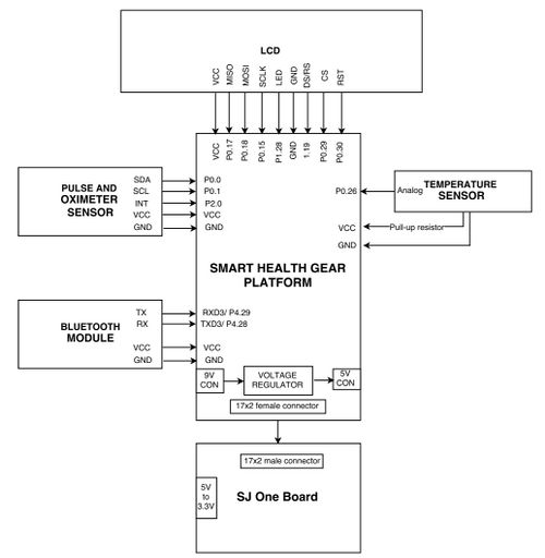
Hardware Interface Diagram
Heart Rate Sensor
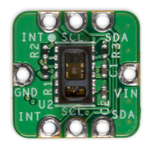
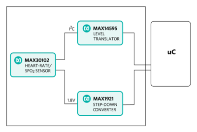
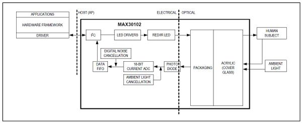
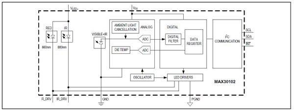
The Heart-Rate Monitor and Pulse Oximeter Sensor (MAXREFDES117) design is a Photoplethysmogram (PPG) based heart-rate and SpO2 monitor subsystem. The module contains heart-rate/SpO2 sensor (MAX30102), a low-power step-down converter (MAX1921), and a level translator (MAX14595). The circuit utilizes the MAX30102 heart-rate/SpO2 sensor with integrated red and IR LEDs to detect heart rate and pulse ox on a person’s fingertip, earlobe. It should be powered on using a 2V to 5.5V supply. The step-down converter MAX1921 converts the 2V to 5.5V supply input and generates the 1.8V rail for the heart-rate sensor. The MAX14595 level translator provides an interface between the heart-rate/SpO2 sensor and the controller board, which generally use a different logic level.
It can be interfaced with using I2C communication and is fully adjustable through software registers, and the digital output data can be stored in a 32-deep FIFO within the IC. The SDA(P0.0) and SCL(P0.1) are connected on the I2C1 of the SJ-one board and interrupt is connected to GPIO pin on port 2 (P2.0) as shown on interface diagram. An interrupt is generated whenever it the FIFO gets filled and the samples are read as it gets filled.
Due to the form factor of the IC it is ideal for wearable and it is can be clipped on to the finger of the person.
Temperature Sensor
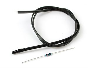
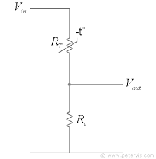
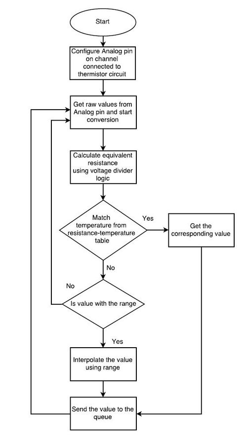
A NTC thermistor is used to compute the body temperature connected to the analog pin of the SJ-one board. A volatge divider circuit is connectd acrcoss the analog pin of the board. A 10K resistor and thermistor are used in voltage divider circuit whose Vout is connected to analog pin as shown in figure. Now you just measure the voltage in the middle, as the resistance changes, the voltage changes too, according to the simple voltage-divider equation.
Hardware Features
- Resistance at 25 degrees C: 10K +- 1%
- B25/50 = 3950+- 1%
- Thermal time constant <= 15 seconds
- Thermistor temperature range -55 °C to 125 °C
- 28 AWG PVC Wire
LCD
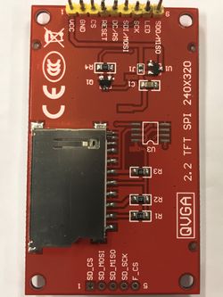
Features:
- Display resolution: [240xRGB](H) x 320(V)
- Output:
- 720 source outputs
- 320 gate outputs
- a-TFT LCD driver with on-chip full display RAM: 172,800 bytes
- System Interface
- 3-line / 4-line serial interface [SPI/I2C
- Display mode:
- Full color mode (Idle mode OFF): 262K-color
- Reduce color mode (Idle mode ON): 8-color
- On chip functions:
- VCOM generator and adjustment
- Timing generator
- Oscillator
- DC/DC converter
- Line/frame inversion
- 4 preset Gamma curves with separate RGB Gamma correction
Software Features
- Uses SPI interface to connect to the LCD
- The LCD interface is initialized by sending commands to set the power, frame rate, pixel depth etc.,
- The LCD screen is filled up pixel by pixel depending on what to display
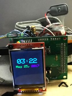
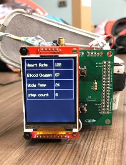
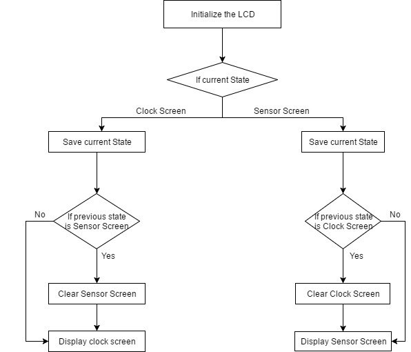
- Alternates between two screens - the Default Screen in which timer displays the current time and Sensor Screen which shows the data collected from all the sensors
- Captures data continuously and displays whenever neccessary
- There are two switches using which the user can turn on/off the LCD
- The user can also swap the screens by pressing the Sensor Screen button
- The timer will ensure that the sensor screen will swap back to the Timer screen after counting 300 times
To display characters or lines or any shapes we need to fill up the screen pixel by pixel by positioning the pixels in appropriate location using the row set and column set commands. The commands and its parameters are sent to LCD via SPI interface and are then followed by the data i.e., the pixel color.
There are two screens – The default screen will display the Time Stamp and the next screen will display the sensor data. These two screens are swapped either after timeout or after a button press. A timer is initialized to count every micro second and after counting 300 times the timer gives a binary semaphore which is captured a task which swaps the screens. The LCD is interfaced to two switches using two GPIO pins. One switch is used to power off and power on the LCD and the other one is used to navigate between the two screens.
HC-05 Bluetooth Module
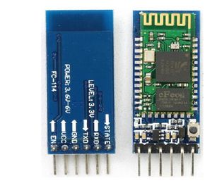
HC-05 module is an easy to use Bluetooth SPP (Serial Port Protocol) module, designed for transparent wireless serial connection setup. Serial port Bluetooth module is fully qualified Bluetooth V2.0+EDR (Enhanced Data Rate) 3Mbps Modulation with complete 2.4GHz radio transceiver and baseband. It uses CSR Bluecore 04-External single chip Bluetooth system with CMOS technology and with AFH(Adaptive Frequency Hopping Feature). It has the footprint as small as 12.7mmx27mm.
Hardware Features
- Typical -80dBm sensitivity
- Up to +4dBm RF transmit power
- Low Power 1.8V Operation, 1.8 to 3.6V I/O
- PIO control
- UART interface with programmable baud rate
- With integrated antenna
- With edge connector
Software Features
- Default Baud rate: 38400, Data bits:8, Stop bit:1,Parity:No parity, Data control: has.
Supported baud rate: 9600,19200,38400,57600,115200,230400,460800.
- Given a rising pulse in PIO0, device will be disconnected.
- Status instruction port PIO1: low-disconnected, high-connected;
- PIO10 and PIO11 can be connected to red and blue led separately. When master and slave
are paired, red and blue led blinks 1time/2s in interval, while disconnected only blue led blinks 2times/s.
- Auto-connect to the last device on power as default.
- Permit pairing device to connect as default.
- Auto-pairing PINCODE:"1234" as default
- Auto-reconnect in 30 min when disconnected as a result of beyond the range of connection.
Software Design
Show your software design. For example, if you are designing an MP3 Player, show the tasks that you are using, and what they are doing at a high level. Do not show the details of the code. For example, do not show exact code, but you may show pseudocode and fragments of code. Keep in mind that you are showing DESIGN of your software, not the inner workings of it.
Body Temperature Calculation
Thermistor is connected to the analog pin across a voltage-divider circuit using a 10K resistor. Now you just measure the voltage in the middle, as the resistance changes, the voltage changes too, according to the simple voltage-divider equation. Based on the resistance value we can find the corresponding temperature value by matching it with the look-up table provided by the vendor.
Heart rate calculation
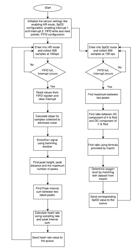
- The heart rate (bpm) is calculated by sensing the photoplethysmograph signal from the Pulse and Oximeter Sensor. By connecting the sensor on the I2C interface we
get the raw values and collect about 100 samples every second.
- Initialize the sensor settings like enabling HR mode, SpO2 configuration, interrupt 1 and interrupt 2, FIFO write and read pointer, FIFO configuration by writing
appropriate values into the registers as specified in the datasheet.
- The raw values contain noise as well so it is eliminated by finding derivative of the signal. For this purpose, we find the slope of the signal which would be
series of either positive or negative number.
- To this derivative signal, a hamming window is applied to smoothen out all edges and the signal is like a sine wave.
Software flowchart:
Algorithm Pseudocode:
- Read values from FIFO register whenever an interrupt occurs.
- Continuously take samples from MAX30102. The heart rate and SpO2 are calculated for every 1 second.
- Eliminate the first 100 samples from the register and calculate for every 500 samples by sliding the frame as samples occur.
- Find moving average of the sample raw values i.e slope calculation
- Apply hamming window to the signal with window size as 5.
- Find peak height, peak distance and the maximum number of peaks.
- Find at most MAX_NUM peaks above MIN_HEIGHT separated by at least MIN_DISTANCE
- If the number of peaks < 2, find peak interval sum.
- Find the peak interval sum = time of the last peak – time of next peak.
- Based on the sampling rate, calculate the heart rate 6000/ peak interval sum and loop back to finding the peak.
- For SpO2 calculation, we need to assess DC and AC value of IR and red PPG.
- Find maximum between two peaks and use the ratio between AC component of Ir & Red and DC component of Ir & Red for SPO2.
- The accurate SPO2 is precalculated and save in uch_spo2_table[] per each ratio
- Ratio = -45.060*n_ratio_average* n_ratio_average/10000 + 30.354 *n_ratio_average/100 + 94.845
- Match the ratio as per the values in the table to get the correct SPO2 value.
Android Application
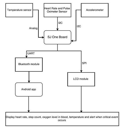
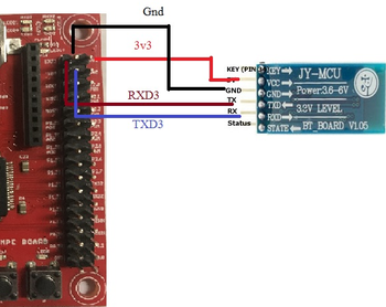
Development of the Android application is done using Android Studio Version 2.3.2. The application is connected to the HC-05 Bluetooth module using Bluetooth module. The HC-05, in turn, is interfaced with the SJOne board using Uart3 at the baud rate of 9600 bps. The connections are shown below. The data is sent to the module using serial communication nearly after every second and the value is simultaneously updated on the mobile application.
Android Studio is Android's official IDE. It offers tools custom-tailored for Android developers, including rich code editing, debugging, testing, and profiling tools. The Android app is built using 4 basic files namely AndroidManifest.xml, DeviceListActivity.java, MainActivity.java and activity_main.xml. Every application must have an AndroidManifest.xml file (with precisely that name) in its root directory. The manifest file provides essential information about your app to the Android system, which the system must have before it can run any of the app's code.
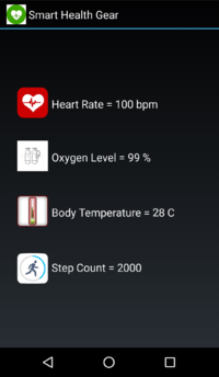
The layout of the Application has four text boxes to display the four different parameters of data i.e. Heart Rate, Body Oxygen Level, Body Temperature and Step Count.
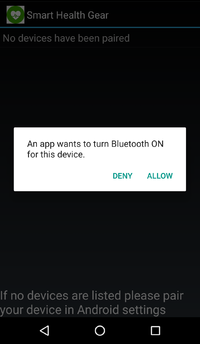
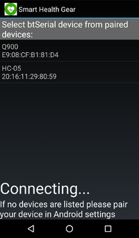
Upon opening the Application, if the Bluetooth connection of the Phone is not ON, the app will request permission to turn on Bluetooth. The first page of the application will display all the paired devices with the Phone.
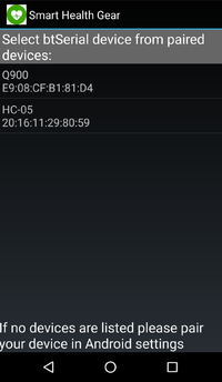
After selecting HC-05 among the list of paired devices, the app will connect to the module HC-05 and is ready to receive data from the module.
All the four parameters are passed in the format shown below:
Uart3& uart_3 = Uart3::getInstance();
uart_3.init(9600);
uart_3.printf("#%3d+%3d+%3d+%4d+~",heartRate, bodyOxygen, bodyTemp, stepCount);
On the application side, the above-received string is parsed accordingly to extract the value of each parameter and display it in the appropriate text box.
if (recDataString.charAt(0) == '#')		              //if it starts with # we know it is what we are looking for
{
  String sensor0 = recDataString.substring(1, 4);             //get sensor value from string between indices 1-5
  String sensor1 = recDataString.substring(5, 8);             //same again...
  String sensor2 = recDataString.substring(9, 12);
  String sensor3 = recDataString.substring(13, 17);

  sensorView0.setText(" Heart Rate = " + sensor0 + " bpm");	//update the textviews with sensor values
  sensorView1.setText(" Oxygen Level = " + sensor1 + " %");
  sensorView2.setText(" Body Temperature = " + sensor2 + " C");
  sensorView3.setText(" Step Count = " + sensor3 + "");
}
Implementation
This section includes implementation, but again, not the details, just the high level. For example, you can list the steps it takes to communicate over a sensor, or the steps needed to write a page of memory onto SPI Flash. You can include sub-sections for each of your component implementation.
Testing & Technical Challenges
Describe the challenges of your project. What advise would you give yourself or someone else if your project can be started from scratch again? Make a smooth transition to testing section and described what it took to test your project.
Include sub-sections that list out a problem and solution, such as:
My Issue #1
Discuss the issue and resolution.
Conclusion
Conclude your project here. You can recap your testing and problems. You should address the "so what" part here to indicate what you ultimately learnt from this project. How has this project increased your knowledge?
Project Video
Upload a video of your project and post the link here.
Project Source Code
References
Acknowledgement
Any acknowledgement that you may wish to provide can be included here.
References Used
List any references used in project.
Appendix
You can list the references you used.
