Difference between revisions of "F16: OBD2 Reader"
146 user15 (talk | contribs) (→Implementation) |
146 user15 (talk | contribs) (→CAN Bus) |
||
| (22 intermediate revisions by the same user not shown) | |||
| Line 41: | Line 41: | ||
| − | The CAN Bus data message frame is composed of a Starting Frame, an Arbitration Field, a Control Field, Data Field, Cyclic Redundancy Check, Acknowledge Field, and an End of Frame. The Starting Frame is used to indicate the start of a message when bit is zero. The Arbitration Field is used to define the message priority. The Control Field is used to describe the length of the data being sent. The Data Field is used to send the actual payload to the other CAN nodes. The Cyclic Redundancy Check is used to detect any errors in the data. The Acknowledge Field is used to let the transmitter know that | + | The CAN Bus data message frame is composed of a Starting Frame, an Arbitration Field, a Control Field, Data Field, Cyclic Redundancy Check, Acknowledge Field, and an End of Frame. The Starting Frame is used to indicate the start of a message when the bit is zero. The Arbitration Field is used to define the message priority. The Control Field is used to describe the length of the data being sent. The Data Field is used to send the actual payload to the other CAN nodes. The Cyclic Redundancy Check is used to detect any errors in the data. The Acknowledge Field is used to let the transmitter know that the data was successfully received. The End of Frame is used to indicate the end of the data. |
| − | In the CAN system, there is no control host. When a CAN node is about to send data into the bus it first checks to see if the bus is busy. If the bus is not busy, the CAN node will send a message frame to the bus. The message frame does not contain a destination address so the message frame will be received by all nodes on the bus. Depending on the Arbitration Field, each CAN node will decide if they should ignore or accept the frame. When more than one CAN node tries to send a frame to the BUS at the same time, the node with the lower Arbitration ID will have the higher priority to the bus. The lower priority nodes will have to wait until the higher priority | + | In the CAN system, there is no control host. When a CAN node is about to send data into the bus it first checks to see if the bus is busy. If the bus is not busy, the CAN node will send a message frame to the bus. The message frame does not contain a destination address so the message frame will be received by all nodes on the bus. Depending on the Arbitration Field, each CAN node will decide if they should ignore or accept the frame. When more than one CAN node tries to send a frame to the BUS at the same time, the node with the lower Arbitration ID will have the higher priority to the bus. The lower priority nodes will have to wait until the higher priority node is done. |
== Objectives & Introduction == | == Objectives & Introduction == | ||
| Line 168: | Line 168: | ||
== Parts List & Cost == | == Parts List & Cost == | ||
| − | |||
{| class="wikitable" | {| class="wikitable" | ||
| Line 210: | Line 209: | ||
== Design & Implementation == | == Design & Implementation == | ||
| − | The | + | The following sub-sections describe the hardware and software design configurations that were utilized in this project. |
=== Hardware Design === | === Hardware Design === | ||
| Line 224: | Line 223: | ||
=== Hardware Interface === | === Hardware Interface === | ||
| − | The SJ One board is able to communicate with the vehicle's ECU using the CAN bus protocol. | + | The SJ One board is able to communicate with the vehicle's ECU using the CAN bus protocol. A CAN bus transceiver was connected to the Rx and Tx output pins of the SJ One board so that the signals voltage levels could be converted to CAN bus appropriate levels. The transceiver output CAN High and CAN Low signals are then connected to the DB9 pins of the OBD2 to DB9 adapter so that the CAN High and CAN Low signals can be transmitted to the vehicle's OBD2 port. A 120 ohms resistor was connected to the CAN High and CAN Low on the transceiver's side in order to prevent any signals from reflecting. The other end already contained a 120 ohm resistor in the ECU. |
| − | The OLED display module consists of the actual OLED display along with an SSD1306 controller chip which drives the display. Implementing the OLED module required a thorough understanding of the initialization and communication procedures laid out by the controller chip's datasheet. | + | The OLED display module consists of the actual OLED display along with an SSD1306 controller chip which drives the display. Implementing the OLED module required a thorough understanding of the initialization and communication procedures laid out by the controller chip's datasheet. The SSD1306 acts as a slave device on the I2C bus as it communicates with the SJ One board master device. The SJ One board writes to a series of registers on the SSD1306 to control the display. |
| − | |||
| − | The SSD1306 acts as a slave device on the I2C bus as it communicates with the | ||
=== Software Design === | === Software Design === | ||
| Line 255: | Line 252: | ||
* OLED Display Implementation | * OLED Display Implementation | ||
| + | |||
A series of commands must be issued to the SSD1306 in order to prepare the display for operation. The commands are issued as a series of register writes over the I2C bus from the SJ One board master device to the SSD1306 slave device. The registers that are to be written to for implementing the initialization sequence are shown in the following table: | A series of commands must be issued to the SSD1306 in order to prepare the display for operation. The commands are issued as a series of register writes over the I2C bus from the SJ One board master device to the SSD1306 slave device. The registers that are to be written to for implementing the initialization sequence are shown in the following table: | ||
{| class="wikitable" style="margin: auto;" | {| class="wikitable" style="margin: auto;" | ||
| Line 309: | Line 307: | ||
| Turn the display on | | Turn the display on | ||
|} | |} | ||
| + | |||
| + | The following diagram shows the functions utilized in the initialization sequence of the display driver. First, the I2C protocol is initialized in order to set up the communication between the SJ One board and the OLED display. Afterwards, the initial contents of the buffer are displayed to the screen. The buffer initially contains a bitmap image of the Adafruit Logo, this splash screen image is to be displayed upon boot up as requested by the manufacturer. The process of writing the buffer to the display consists of of sending each entry in the buffer to the display over the I2C bus. After some time delay, the display splash screen is cleared and the display becomes ready for interfacing. | ||
| + | |||
| + | [[File:CmpE146_F16_G1_OLEDSWInit.png|center|720 px|thumb|Figure 11. OLED display software initialization sequence]] | ||
| + | |||
| + | The following diagram shows the functions utilized in the writing sequence of the display driver. First, the display is prepared for the writing sequence through a series of register writes. The purpose of these register writes is to configure the rows and columns that are to be used by the display. Afterwards, the string is dissected and saved to the buffer. Finally, the buffer is written to the display one character at a time over the I2C bus. | ||
| + | |||
| + | [[File:CmpE146_F16_G1_OLEDSWDisplay.png|center|thumb|Figure 12. OLED display writing sequence]] | ||
* Memory Unit | * Memory Unit | ||
| Line 317: | Line 323: | ||
message is written. Alternatives to this approach entail using the on-board memory. | message is written. Alternatives to this approach entail using the on-board memory. | ||
| − | [[File:CMPE146_F16_G1_SDCard.jpg|center| | + | [[File:CMPE146_F16_G1_SDCard.jpg|center|thumb|Figure 13. SD Card]] |
== Testing & Technical Challenges == | == Testing & Technical Challenges == | ||
| Line 351: | Line 357: | ||
=== Project Source Code === | === Project Source Code === | ||
* [https://sourceforge.net/projects/sjsu/files/CmpE_S2016/ Sourceforge Source Code Link] | * [https://sourceforge.net/projects/sjsu/files/CmpE_S2016/ Sourceforge Source Code Link] | ||
| − | * [https://github.com Github Project Repository] | + | * [https://github.com/cmpe146f16g1/OBD2Reader Github Project Repository] |
=== Video === | === Video === | ||
| − | * [https://www.youtube.com/watch?v=yAEXL-Hv8nQ Demo | + | * [https://www.youtube.com/watch?v=yAEXL-Hv8nQ Video Demo] |
== References == | == References == | ||
| Line 365: | Line 371: | ||
=== References Used === | === References Used === | ||
| − | + | ||
| + | * [http://www.socialledge.com/sjsu/index.php?title=CAN_BUS_Tutorial CAN Bus Tutorial] | ||
=== Appendix === | === Appendix === | ||
| − | |||
* [http://www.ti.com/lit/ds/symlink/sn65hvda1040a-q1.pdf SN65HVDA1040 CAN Transceiver Datasheet] | * [http://www.ti.com/lit/ds/symlink/sn65hvda1040a-q1.pdf SN65HVDA1040 CAN Transceiver Datasheet] | ||
* [https://cdn-shop.adafruit.com/datasheets/SSD1306.pdf OLED Display Datasheet] | * [https://cdn-shop.adafruit.com/datasheets/SSD1306.pdf OLED Display Datasheet] | ||
Latest revision as of 01:59, 21 December 2016
Contents
Abstract
This project entails the use of can bus structure to create a form of communication between our Microcontroller and a vehicle's ECU. Once connected using this protocol, our Microcontroller using the Can controller will interface with the ECU and retrieve diagnostic information stored in the ECU for debbuging. Once these codes are stored in our memory location on the Microcontroller, we will reset the diagnostic data of the ECU and clear the check engine on the car. using a transceiver and OBD2 protocol. The OBD2 codes retrieved from the vehicle are compared to the Microcontroller's database. If there is a match, a corresponding message is displayed to the user via an LCD screen. The LCD screen will use the I2C protocol to transmit the data from our Microcontroller to the LCD screen. These messages will entail diagnostic data and instructions.
OBD2 Reader
On-board vehicle diagnostics (OBD) refers to an interface that connects to a vehicle's computer and allows the vehicle to self-diagnose problems and report them. OBD-II or OBD2 is an OBD standard which the type of connector, messaging format, electrical signaling, and a list of other vehicle parameters.
The OBD2 reader is an on board diagnostic device that translates the diagnostic code from a vehicle's engine control unit (ECU) to comprehensible data for the user. This device employed several protocols from CMPE 146 lab and techniques taken from the Socialledge Wiki to implement the design. The cars onboard ECU takes all the sensory data from several sensors and units and translates it into hexadecimal numbers that it then outputs its OBD2 port. Our OBD2 ready device links with the car’s ECU and reads diagnostic information from it, which it then transmits to the microcontroller which in turn compares the information to its database codes and print a message that explains what the code means. If the codes from the ECU match the code stored on our board, the board will display the result on Hercules and an LCD device that was configured with out system. The LCD device was implemented on top of our board using the I2C protocol; it display the error message corresponding to the vehicle's obd code as well as diagnostic suggestions and further steps to take.
CAN Bus
Controlled Area Network (CAN Bus) Bus is a message-based protocol used by all vehicles. CAN bus allows devices and Microcontrollers to communicate without a host machine. Several different devices can be interfaced to CAN Bus, such as the control unit for the airbags, an anti-lock braking system, the power steering system, a proximity sensor, and the OBD2 connector.
The CAN Bus is made up of two wires, CAN-H (CAN High) and CAN-L (CAN Low). Both wires connect to all devices on the bus. A signal is transmitted as a differential pair of signals on its own wire. When the CAN-H wire receives a signal, the CAN-L wire also receives the same signal but with an opposite amplitude. The reason for this is to reduce the chance of data corruption by making it less vulnerable to noise. The CAN-H wire can go from 2.5V to 3.75V and the CAN-L wire can go from 2.5V down to 1.25V.
When the CAN Bus is implemented on a vehicle, both CAN-H and CAN-L wires must be twisted together with two 120 Ohm terminating resistors. By having the wires twisted together, they are able to eliminate any noise. The two terminating resistors are connected to both ends of the bus to eliminate any signals from reflecting. In Figure 2, Device 1 denotes the LPC1758 Microcontroller and Device n denotes a transceiver. Device n is required as the RX and Tx pins from the Microcontroller send out logical signals that need to be converted to a single differential pair which connects to the OBD2 port.
The CAN bus system has two different formats for the message frame, 2.0A and 2.0B. The difference is that 2.0A is the standard and uses 11 bits in the arbitration field, and 2.0B is the extended version and uses 29 bits in the arbitration field.
The CAN Bus data message frame is composed of a Starting Frame, an Arbitration Field, a Control Field, Data Field, Cyclic Redundancy Check, Acknowledge Field, and an End of Frame. The Starting Frame is used to indicate the start of a message when the bit is zero. The Arbitration Field is used to define the message priority. The Control Field is used to describe the length of the data being sent. The Data Field is used to send the actual payload to the other CAN nodes. The Cyclic Redundancy Check is used to detect any errors in the data. The Acknowledge Field is used to let the transmitter know that the data was successfully received. The End of Frame is used to indicate the end of the data.
In the CAN system, there is no control host. When a CAN node is about to send data into the bus it first checks to see if the bus is busy. If the bus is not busy, the CAN node will send a message frame to the bus. The message frame does not contain a destination address so the message frame will be received by all nodes on the bus. Depending on the Arbitration Field, each CAN node will decide if they should ignore or accept the frame. When more than one CAN node tries to send a frame to the BUS at the same time, the node with the lower Arbitration ID will have the higher priority to the bus. The lower priority nodes will have to wait until the higher priority node is done.
Objectives & Introduction
This project aims to design an OBD2 reader using the SJOne LPC 1758 board. The reader will display a vehicle's Engine Control Unit (ECU) information via an OLED screen.
Objectives:
- Interface the SJOne board with the OBD2 reader
- Store and read external memory module through SJOne board
- Interfacing SJOne to external OLED display
Sensors and Peripherals Used:
- ECU (information source device)
- SJOne (for processing information)
- External Memory and Memory Interface
- OLED (display vehicle diagnostics)
Team Members & Responsibilities
- R Nikfar
- Electrical Engineering Advising, Can Bus protocol Design, Eagle PCB design, Electrical Components, Firmware Coding, and Mechanical Engineering sensor and Component Debugging.
- Samira Oliva
- CAN Driver Programming and Setting up the memory unit.
- Samuel Palomino
- CAN Driver Programming, OLED Display Driver Programming and Component Debugging.
- Erik Sanchez
- Setting up the memory unit.
Schedule
| Week # | Start Date | End Date | Planned Tasks | Status | Actual Outcome |
|---|---|---|---|---|---|
| 1 | 10/30/16 | 11/05/16 |
|
Completed |
|
| 2 | 11/06/16 | 11/12/16 |
|
Completed | Completed |
| 3 | 11/13/16 | 11/19/16 |
|
Completed | Completed |
| 4 | 11/20/16 | 11/26/16 |
|
Completed | Completed |
| 5 | 11/27/16 | 12/03/16 |
|
Completed | Completed |
| 6 | 12/04/16 | 12/10/16 |
|
Completed | Completed |
| 7 | 12/11/16 | 12/17/16 |
|
Completed | Completed |
| 8 | 12/18/16 | 12/20/16 |
|
Completed | Completed |
Parts List & Cost
| Item | Qty. | Price (Total) | Vendor | Description |
|---|---|---|---|---|
| SJOne Board | 1 | $80.00 | SJSU | SJOne board |
| CAN Transceiver | 1 | $1.68 | Mouser | Handles CAN bus signals voltage conversion |
| OBD2 to DB9 Adapter | 1 | $6.99 | Amazon | Connects the vehicle's ECU to SJOne board |
| OLED Display | 1 | $9.99 | Amazon | I2C 128x64 Display Module |
Design & Implementation
The following sub-sections describe the hardware and software design configurations that were utilized in this project.
Hardware Design
Our system consists of four major components: the SJ One board, the CAN bus transceiver, the vehicle's ECU and an OLED display. In order for the SJ One board to successfully communicate with the vehicle's ECU over the CAN bus, a CAN bus transceiver was required. The OLED display acts a simple visual aid to help the user visualize what commands are being sent and what data is being received.
Hardware Interface
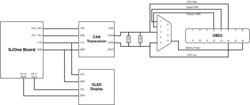
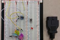
The SJ One board is able to communicate with the vehicle's ECU using the CAN bus protocol. A CAN bus transceiver was connected to the Rx and Tx output pins of the SJ One board so that the signals voltage levels could be converted to CAN bus appropriate levels. The transceiver output CAN High and CAN Low signals are then connected to the DB9 pins of the OBD2 to DB9 adapter so that the CAN High and CAN Low signals can be transmitted to the vehicle's OBD2 port. A 120 ohms resistor was connected to the CAN High and CAN Low on the transceiver's side in order to prevent any signals from reflecting. The other end already contained a 120 ohm resistor in the ECU.
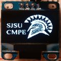
The OLED display module consists of the actual OLED display along with an SSD1306 controller chip which drives the display. Implementing the OLED module required a thorough understanding of the initialization and communication procedures laid out by the controller chip's datasheet. The SSD1306 acts as a slave device on the I2C bus as it communicates with the SJ One board master device. The SJ One board writes to a series of registers on the SSD1306 to control the display.
Software Design
The program consists of a CAN task class derived from the scheduler_task class. This class is used to configure a driver for the CAN protocol. This single task takes care of preparing the bus for communication and also the message transmission and reception. First, the CAN bus is initialized. Then, the CAN bus is set up so that all messages on the bus are received. There is no need to filter the messages traveling on the CAN bus as there are only two devices on our bus. Finally, the CAN bus is reset so that it's ready for communication. This concludes the set up portion of the CAN bus.
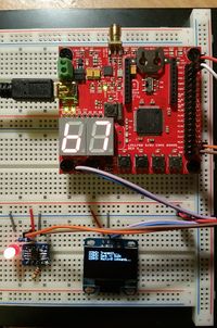
Additionally, the program communicates with an external OLED display to easily see which CAN messages are being sent and received. Doing so allowed for ease of verifying what data is being sent and received by the system. The OLED display is directly interacted with through the single task in our program since the display contents rely on the CAN bus data.
- Communication Protocols:
- Controller Area Network (CAN)
- Communicates with the vehicle's ECU.
- I2C
- Communicates with the OLED display.
- Controller Area Network (CAN)
Implementation
- CAN Implementation
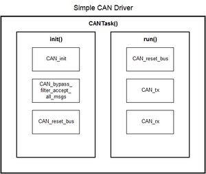
The following diagram shows the overall flow of actions in the CAN driver: initializing the CAN Bus, filter settings, reset, and the task running that consists of bus resetting, transmission, and reception.
- OLED Display Implementation
A series of commands must be issued to the SSD1306 in order to prepare the display for operation. The commands are issued as a series of register writes over the I2C bus from the SJ One board master device to the SSD1306 slave device. The registers that are to be written to for implementing the initialization sequence are shown in the following table:
| Register | Command Description |
|---|---|
| 0xAE | Turn the display off |
| 0xD5 | Set SSD1306 oscillator frequency |
| 0xA8 | Set MUX Ratio |
| 0xD3 | Set display offset |
| 0x40 | Set display start line |
| 0x8D | Set SSD1306 to be powered by the module's regulator |
| 0x20 | Set horizontal addressing mode |
| 0xA0 | Set columns to be mapped to display segments |
| 0xC0 | Set COM scan from top to bottom |
| 0xDA | Set COM pins hardware configuration |
| 0x81 | Set contrast control |
| 0xD9 | Set pre-charge period |
| 0xDB | Set Vcom deselect level |
| 0xA4 | Set display to replicate contents in RAM |
| 0xA6 | Set display to normal (no color inversion) |
| 0xAF | Turn the display on |
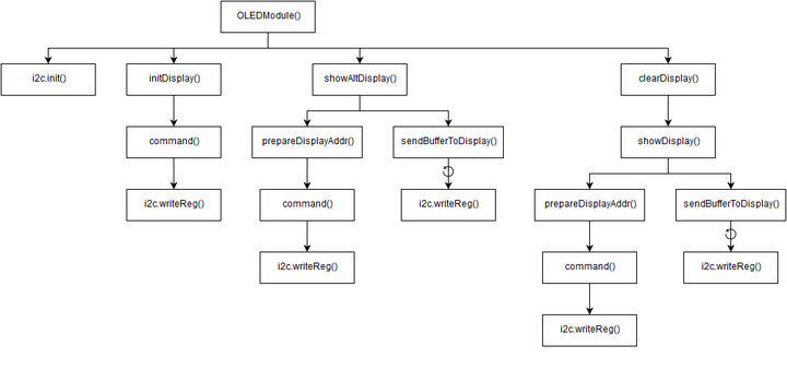
The following diagram shows the functions utilized in the initialization sequence of the display driver. First, the I2C protocol is initialized in order to set up the communication between the SJ One board and the OLED display. Afterwards, the initial contents of the buffer are displayed to the screen. The buffer initially contains a bitmap image of the Adafruit Logo, this splash screen image is to be displayed upon boot up as requested by the manufacturer. The process of writing the buffer to the display consists of of sending each entry in the buffer to the display over the I2C bus. After some time delay, the display splash screen is cleared and the display becomes ready for interfacing.
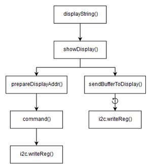
The following diagram shows the functions utilized in the writing sequence of the display driver. First, the display is prepared for the writing sequence through a series of register writes. The purpose of these register writes is to configure the rows and columns that are to be used by the display. Afterwards, the string is dissected and saved to the buffer. Finally, the buffer is written to the display one character at a time over the I2C bus.
- Memory Unit
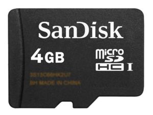
An SD card was used to store a file containing OBDII codes. This was necessary in order to perform file IO and process the codes in an array. The array used by the driver to search for a tranmitted OBD code. If found, the corresponding message is written. Alternatives to this approach entail using the on-board memory.
Testing & Technical Challenges
Describe the challenges of your project. What advise would you give yourself or someone else if your project can be started from scratch again? Make a smooth transition to testing section and described what it took to test your project.
Include sub-sections that list out a problem and solution, such as:
Issue #1
The first issue that was encountered involved the memory unit. For this project, we planned to use an AT45 IC FLASH 64MBIT 85MHZ memory. After connecting the memory module to the LPC1758, we created a text file containing the DTCs (Diagnostic Trouble Code) and tried to open the file using Eclipse and transfer the data onto the AT45. After spending days trying to that, we sought to advise of the lab assistant, Praveen. We were informed that we would not be able to open the file and transfer the data to the AT45. If we wanted to transfer data, we would have to type the code and every DTC on the Eclipse IDE, which would take too much time to do because there are about 76 pages of DTCs. Instead, we transferred the text file with the DTCs on the micro SD card and inserted the card on the LPC1758. We later learned that we did not need all the DTCs. We only chose a few DTCs which were able to be stored on the LPC1758's onboard memory.
Issue #2
The second Issue included the lack of information regarding the architecture of the can bus protocol. we originally connected the Tx, Rx from The Microcontroller directly to the can bus Hi and Lo Signals. After several days of troubleshooting, we realized that there would be a need for the specific transceivers(automotive). These transceivers would operate at a much higher frequency than our previous transceivers(500kbps).
Issue #3
After much research, it was determined that the maximum speed of the Microcontroller would not be enough for the Automotive can bus architecture. The Microcontroller's stable speed(100kbps) was much lower than automotive(500kbps). In order to fix this problem, and outside crystal was connected to the board Xtal pin.
Issue #4
Once the physical connection with the vehicle was made and hexadecimal messages were being sent through the can bus, we ran into another issue. The connectors on the J2284 or OBD2 pin to the ECU were not properly marked. This was the most vexing of all the issues due to the ambiguous nature of the problem. We trouble shooted the board, the signal and ultimately were able to narrow the problem down to wrong connection labels(manufacturer error).
Issue #5
Our last problem entailed the implementation of the software. Using given structure of the can bus we were able to create a task and store and transmit values that were not intended. This was mostly due to a wrong implementation of a function designed to convert the values of from the controller to memory. The external memory implementation was removed, and we were able to get the right hex code outputs on the Hercules terminal.
Conclusion
This project vastly improved our understanding of the LPC1758 Can Controller, Can bus architecture, Automotive standards, PID's, I2C standard, LCD interfacing, and Configuration of the Can system. This project ultimately helped our team understand several topics not mentioned in this class, and further prepared each team member to understand the troubleshooting procedures necessary when dealing with an automotive vehicle. The team was successful in retrieving the diagnostic codes from the designated vehicle and reset the check engine light of the vehicle. Our goal for the future is to create a pragmatic device that could be used to interface with a software application or platform.
Project Source Code
Video
References
Acknowledgement
- Many thanks to Praveen Prabhakaran, CMPE 146 lab TA for assisting us with questions in regards to File IO
with the LPC and CAN Bus.
- Many thanks to Professor Kang, CMPE 146 lab instructor for teaching us the fundamentals of embedded systems
programming.


