Difference between revisions of "F12: Smart Bulb"
(→Startup Manager (Conductor / System Engine)) |
(→Shared-Intelligence Network Manager (siNetworkMgr)) |
||
| Line 325: | Line 325: | ||
This task is necessary, as Bulb Logic must be able to respond to both internal and external (network-based) events. To facilitate this requirement, the siNetworkMgr task sends external events to the Bulb Logic task processing queue, while other components, including interrupts and the ambient-light sampling task, send internal events to the processing queue. | This task is necessary, as Bulb Logic must be able to respond to both internal and external (network-based) events. To facilitate this requirement, the siNetworkMgr task sends external events to the Bulb Logic task processing queue, while other components, including interrupts and the ambient-light sampling task, send internal events to the processing queue. | ||
| + | |||
| + | [[File: CmpE146 F12 T2 siMsgPath.png|center|x200px|frame|Message Path for Shared Intelligence Network Messages]] | ||
====== Ambient Sampling ====== | ====== Ambient Sampling ====== | ||
Revision as of 11:14, 20 December 2012
Contents
- 1 SmartBulb: The Intelligent Lighting System
- 2 Abstract
- 3 Objectives & Introduction
- 4 Team Members & Responsibilities
- 5 Schedule
- 6 Parts List & Cost
- 7 Design & Implementation
- 8 Testing & Technical Challenges
- 9 Conclusion
- 10 References
SmartBulb: The Intelligent Lighting System
Problem Statement
Conventional lighting systems do not provide flexibility or automatically adapt to users’ needs. While there has been a push for smarter light bulbs, the equipment which has been released to the market incorporates no intelligence, and the functionality is superficial at best.
Our Solution
A lighting system which adapts to occupant needs and produces optimal light output. SmartBulb automatically recognizes ambient light and the presence of occupants, incorporates the diurnal cycle into its decisions, and enables supervisory devices to request changes to the system configuration.
Abstract
Conventional lighting systems, such as those used in commercial workplaces and residences, are antiquated, primarily because these systems provide minimal flexibility and do not automatically adapt to user’s needs. While there has been a push for “smarter lightbulbs”, the equipment which has been released to the market (such as color configurable LED bulbs) incorporates no intelligence, and the functionality is superficial at best. Being able to change your living room’s color to hot pink via your smartphone only allows a user to amuse him/herself. In comparison, we are interested in having the lighting system adapt to occupant needs automatically, recognizing ambient light and occupant presence, incorporating the diurnal cycle into its decisions, and enabling supervisory devices to request changes to the system’s current configuration.
For instance, each of the bulbs (nodes) within our intelligent lighting system is able to sample the current ambient light within the room without visible interruption to its own light output. This allows us to sample the ambient light using our color sensors, without the light output from the bulb or the adjacent bulbs impacting our measurements. From our samplings, we can determine the intensity of light in the room, along with the color composition of the light. This information is shared amongst all bulbs within the same room via a shared intelligence network facilitated by the Digimesh protocol, which utilizes XBee radios. From this information, a consistent lighting color / temperature is created in the room, and light output can be limited when plenty of ambient light (such as sunlight) is available. When ambient light is limited, the system will utilize the current time-of-day and the diurnal cycle to determine optimal light output. By utilizing the diurnal cycle to make lighting decisions, we can ensure that occupant fatigue due to lighting is minimized, improving occupant comfort.
This project extends the work currently being performed within our senior projects.
Objectives & Introduction
System will be able to detect and adapt to changing ambient light conditions
- If the room is dark and occupants are detected, the system should utilize the time-of-day combined with the diurnal cycle to output the preferred light temperature and brightness
- If the room has ambient light, the system should attempt to match the color of the ambient light and should lower its light output to meet the room’s desired number of lumens.
- For instance, if a warm colored ambient light is visible to the system, it should produce a warm colored output. If a cool color light is visible to the system, it should produce a cool colored output. Extreme cases can also be demonstrated
- Lights should not need to turn on / off (from occupant perspective) during ambient light measurements
- System will be able to respond to supervisory commands via Digimesh network
- Web interface will be connected to Digimesh network via Raspberry Pi or via ConnectPort X2. User will be able to control the current output (intensity, color) of each bulb, and modify other configuration settings (amount time on when occupant detected, relative location to other bulbs, etc.)
- Supervisory commands intended to show that other systems (including home automation) can be tied into this system.
Team Members & Responsibilities
- Phil Cyr
- Hardware architect, electronics, sensors, software
- Stephanie Fung
- Electronics, sensors, software, wiki-updater
- Brandon Schlinker
- Embedded systems architect, software, network
Schedule
| Week Number | Planned Items | Actual |
|---|---|---|
| 1 |
|
|
| 2 |
|
|
| 3 |
|
|
| 4 |
|
|
| 5 |
|
|
| 6 |
|
|
| 7 |
|
|
| Week Number | Scheduled Items | Items Completed |
Parts List & Cost
| Part | Quantity | Unit Cost |
|---|---|---|
| Parallax PIR Motion Sensor | 12.99 | |
| TAOS TCS3414FN Color Sensor | 3.68 | |
| LedEngin LZC-A3MD00 40W RGBW LED Module | 37.70 | |
| LM3404MA High Power LED Driver Chip | 3.28 | |
| LPC1769 Cortex M3 Processor | 9.01 | |
| j-link EDU | 60 | |
| Xbee-PRO DigiMesh 2.4GHz Module | 34 | |
| RN-SMA-S-RP 1" Antenna for Xbee PRO | 5.95 | |
| LS35-5 5V 7A Switching Power Supply | 19 | |
| 36V DC 9.7A 350W Regulated Switching Power Supply | 35.49 | |
| Aavid Heat Sinks 2.25 X 3.0 X 2.996 | 17.25 | |
| Arctic Silver Thermal Cooling Compound | 16.33 |
Design & Implementation
Design
Hardware Design
System Overview
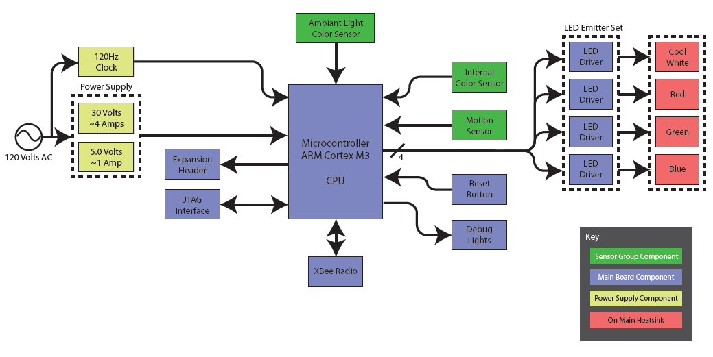
As seen in the main system diagram below, there are four key elements of our system.
Sensor Group Components
The sensors consist of two color sensors and one motion sensor. The techniques for interfacing each individual sensing component is described further into this section. The internal color sensor is soldered directly on the PCB. The other two sensors have extension headers from their respective traces.
Main Board Components
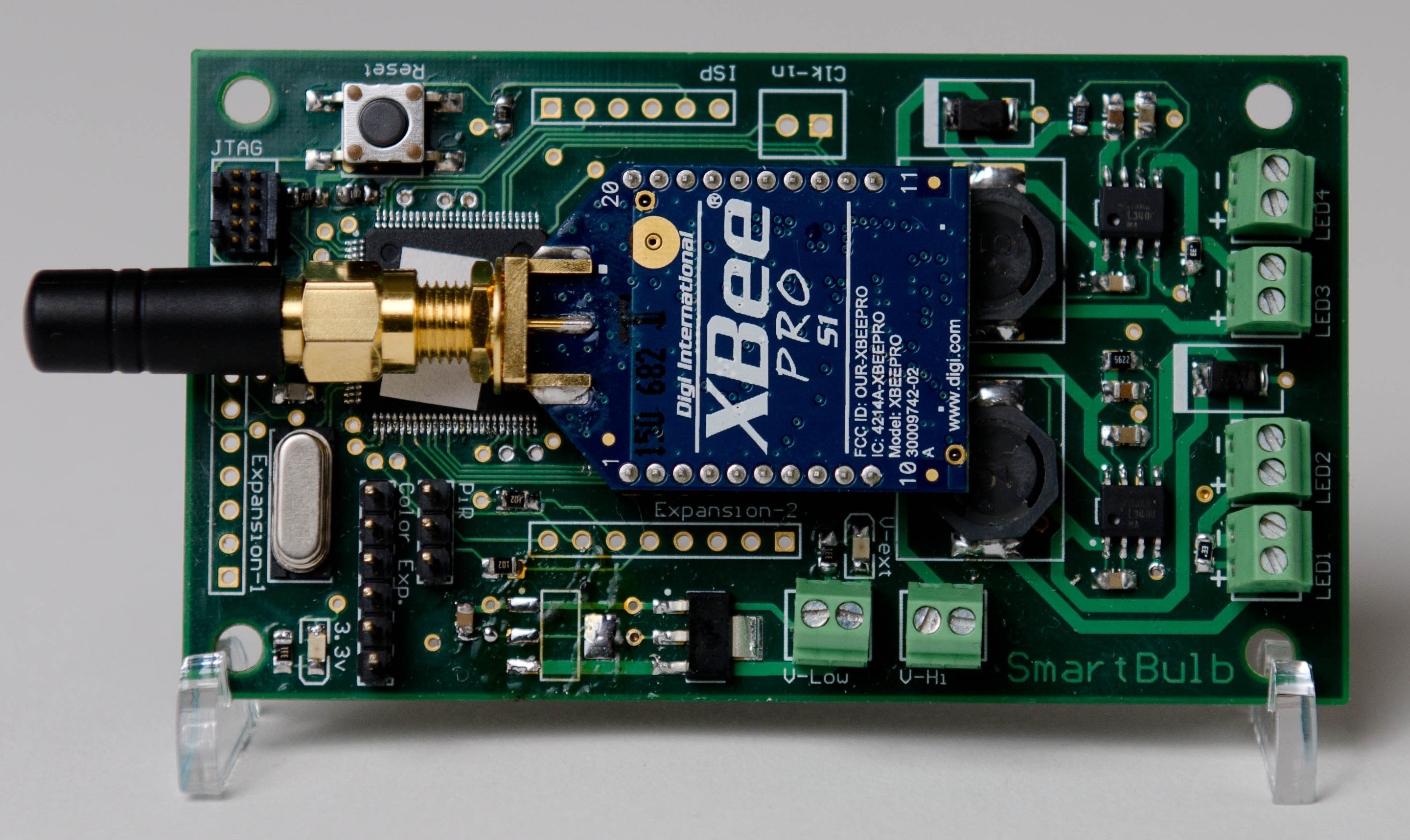
The main board components revolve around our microcontroller. The JTAG interface allows us to flash our microcontoller and debug our code. The debug lights and reset button offer us simple debug tools directly on the PCB. The XBee radio utilizes DigiMesh protocol so that the system can communicate to other light nodes. Furthermore, there are several expansion headers which connect to the microcontroller which allow for expansion and the introduction of new modules.
Power Supply Components
Switching power supply units supply the two main power types used on the board. The 30 volts PSU is utilized by the LED drivers, while the 5 volt power supply supplies the rest of the power.
The LEDs
Our LEDs are driven by the LED drivers which are controlled via pulse-width modulation (PWM). The PWM is software controlled, and the signals are generated by the microcontroller.
Motion Sensing
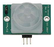
Motion sensing is the key element for the occupancy sensing of the system. This is achieved by using a Parallax PIR motion sensor. There are three pins on the motion sensor: power, ground, and output. The motion sensor is active high, so it will go HIGH (Vcc) when movement is sensed. The approximate distance range for the sensor is 30 feet. By having a motion sensor module on each of lighting fixture, we are able to sense movement to a fine resolution.
Color Sensing
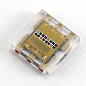
Color sensing on the system consists of two elements: sensing the hue or color, and sensing the brightness or intensity of the light. The main component used to achieve this is the TCS3414, which can sense the intensity of red, green, and blue (RGB) colored light. This color sensor is an I2C device, several photodiodes with corresponding RGB color filters result in different sensor values depending on how much light of each color is sensed on their respective color channels.
Custom PCB
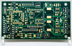
After testing all the components individually on a breadboard, we soon realized that we would need to create a custom PCB in order to achieve the desired form factor for our project. We used Altium as the PCB CAD software to design our board. We designed two iterations of the circuit board. For the first iteration, our goal was to test our design and connections. For the second iteration, we were able to optimize the size based on lessons learned from the board’s first version.
The PCB is split into two sections. The left section is roughly square and contains the embedded system components: CPU, debug interface, radio, control logic, and sensors. The right section, delineated by the large black inductors, contains the power LED driver components.
Microcontroller / Glue Logic
The embedded system portion of the custom PCB provides the computational power to tie the sensors and I/O devices together in the coherent manner that makes them all part of a single system.
The parts were chosen to meet requirements for estimated computational power required as well as manufacturability. Components that only come in a BGA (Ball Grid Array) package were not considered. Components that come in an FN package (Flat No-lead) were avoided. Unfortunately, the color sensor was only available in an FN package. To make the color sensor solderable the land pattern had to be modified. When used in a reflow oven the land pattern for an FN package would not include any copper outside of the chip package footprint, making the packages capable of being placed in close proximity. Without either a lead or a pad extending from the footprint soldering is impossible. Extending the footprint an extra couple millimeters allows the iron to heat the pad and let surface tension pull the solder under the chip.
LED Drivers
The LED drivers represent a critical component in the construction of the SmartBulb. High current LEDs require not only large amounts of power, but regulation of the power consumption. The changes within a single LED between a cold start and running temperature is enough to make efficient constant voltage drive impossible. The PCB contains four single channel drivers, each capable of a constant current drive of 0.7A through up to about 24V of LEDs. The four channels must be independent to provide accurate control of the Red, Green, Blue, and White LEDs in each bulb.
Since the combined forward voltage of the LEDs used is significantly less than the line voltage a buck topology is preferable. A buck converter takes a voltage higher than required and switches it on and off very quickly through a smoothing element to produce the desired output. The output can be either constant voltage or constant current depending on the smoothing element choose. Since the voltage across a capacitor cannot change instantaneously, capacitors are used for constant voltage drive. Similarly since the current through an inductor cannot change instantaneously, inductors are used to produce a constant current drive. The current through the driver is measured with a sense resistor, a small resistor that is used to convert current to voltage without making a significant impact to the circuit. The drivers must drive two 12 volt LEDs in series; a 24 volt load. To keep the required switching frequency within the permissible limits of the drivers, an overhead of about 30% is required in the supply voltage- 36 volts was selected based on the ability to meet the requirements as well as the availability of inexpensive power supplies.
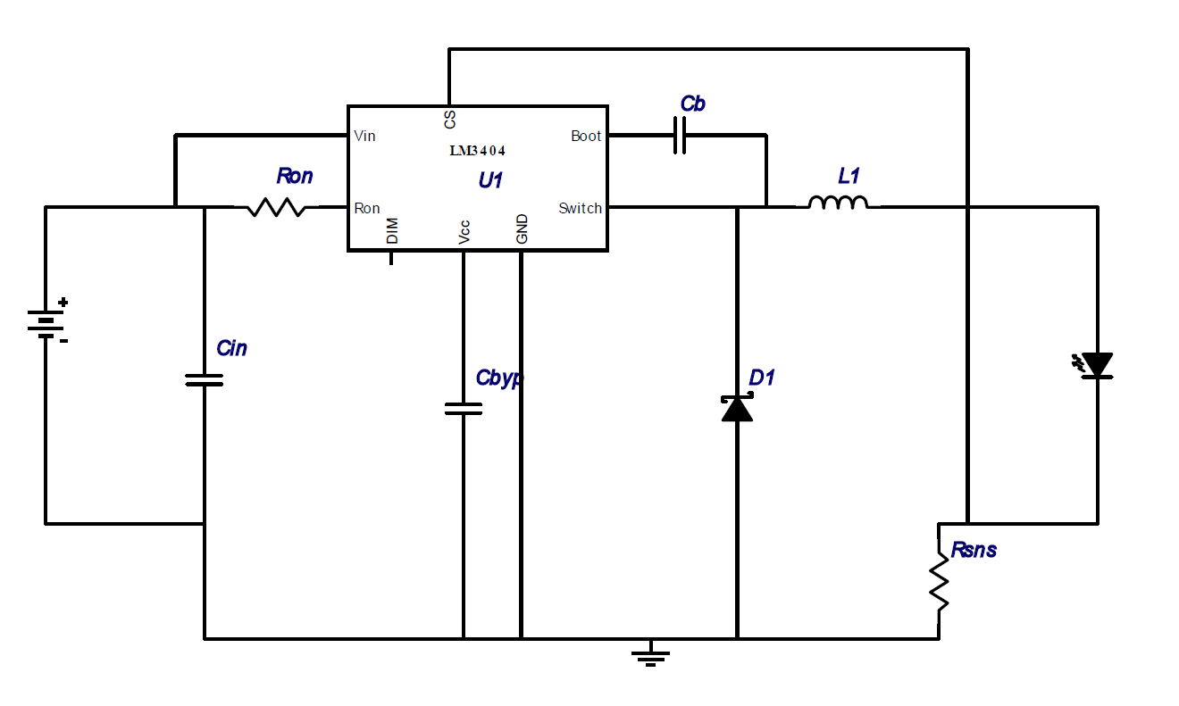
The LED driver design was produced through the use of Texas Instrument's WEBENCH design tool. WEBENCH can suggest power supply and driver designs to meet specified requirements. The selection of the LM3404 was based on the criteria for a chip capable of up to 1A drive, up to 40V supply, and the minimum number of parts required for basic operation. The LM3404 requires only 7 external parts to configure. WEBENCH provides a complete schematic (shown below) and parts list that meets the needs of the user.
Hardware Interface
Disclaimer/Note: Always check the datasheet for the sensor module you are using for the voltage characteristics, rating specifications and pin functions. The interface descriptions shown here are specifically for the parts we used, and should be used as a starting point.
Motion Sensor Connection
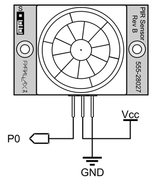
The figure below shows the pin connections for the minimum working circuit to use the PIR motion sensor module.
There are three pins on this specific module from Parallax. The Vcc pin is the supply voltage for the module, which can be 3 to 6 V. The GND pin is connected to ground. The OUT pin is an active high sensor output, it will output a HIGH signal when motion is sensed, and the sensor dome will light up red. We connected this to a pin on our microprocessor to sense motion.
There is a jumper located on the top right of the module. If the jumper is switched to the “S” mode, it will reduce the sensitivity of the sensor to a 15 feet maximum range instead of the 30 feet maximum. We used the sensor in the “L” mode since our application called for maximum sensitivity. When this sensor initially starts up, it has a warm up time of about 40 seconds where the dome will be red and the OUT pin is HIGH. This warm up time is used to allow the sensor to learn the environment, and the datasheet recommends that during this time, there should be as little motion as possible in the sensor’s field of view. Another notable characteristic is that after sensing motion, the OUT pin will remain HIGH for about 1.5 seconds until the sensor will go back to LOW.
Color Sensor Connection
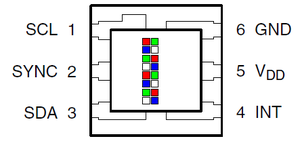
The figure below shows the pin connections for the minimum working circuit to use the color sensor module.
There are six pins on the TCS3414 color sensor module from Taos. The Vcc pin is the supply voltage for the module, which can be 3 to 6 V. The GND pin is connected to ground. SDA and SCL are utilized for I^2^C communication with the sensor, including programming configuration registers and retrieving color data from the sensor registers. The other pins are not needed for standard operation.
PCB Software Design
High-Level System Tasks
Startup Manager (Conductor / System Engine)
The startup manager acts as the system's starting point. After the creation of all RTOS tasks and before the RTOS scheduler is brought online, all tasks except for the startup manager are suspended. As a result, the startup manager is the only task which is executed after the RTOS scheduler is brought online. The startup manager procedurally initializes components within the system engine / conductor, which acts as a central repository of all system resources. If the initialization of any critical component fails, the system will end the startup process, disable the scheduler, and enter a critical failure state.
As each component is successfully initialized, the associated RTOS task (if any) is unsuspended. This enables intercommunication between components as required for system initialization. For instance, the initialization of the Bulb Logic RTOS task is dependent on the Shared-Intelligence Network Supervisor (siNetworkMgr) task being active. As a result, the startup manager will first complete and verify the initialization of the siNetworkMgr task infrastructure, start the siNetworkMgr task, and then proceed to initialize the Bulb Logic task.
The startup manager is critical, as it ensures that inter-task dependencies are handled and verifies the operational integrity of the system prior to boot.
The shared-intelligence network manager pulls for new messages from the XBee API, and then passes received messages to the protobuffer library for decoding / deserializaton. Messages which are successfully decoded by the protobuffer library are then passed into the Bulb Logic task via an RTOS queue. In addition, the siNetworkMgr verifies that the bulb's unique identification address exists within the shared-intelligence network message's recipient field.
This task is necessary, as Bulb Logic must be able to respond to both internal and external (network-based) events. To facilitate this requirement, the siNetworkMgr task sends external events to the Bulb Logic task processing queue, while other components, including interrupts and the ambient-light sampling task, send internal events to the processing queue.
Ambient Sampling
Ambient sampling is achieved synchronously among bulbs via a shared ground-truth. The ambient sampling task waits on a binary semaphore to begin the sampling process. An external interrupt provided the semaphore, which was then used to begin the ambient sampling process. We did not perform the sampling directly within the interrupt, as this would prevent portions of our error-handling code from operating. In addition, the I^2^C driver was interrupt driven and would require modification to operate from within an interrupt (specifically, the driver would need to be modified to support a polling-operation when called from an ISR). To ensure the ambient sampling task completed without interruption, it had a higher priority then the siNetworkMgr and Bulb Logic tasks.
After the ambient sampling process completed, it sent the sampled data to the Bulb Logic task's processing queue. It then waited for the next sampling period by waiting on the binary semaphore.
Bulb Logic
Bulb Logic utilized information from its processing queue to direct the bulb's operation. The processing queue was able to accept different message types by having a single structure which contained unionized, nested structures and a message type parameter. As each message was removed from the queue, the system would check the message type to determine the appropriate nested structure to review. Information from the nested structure was then used to determine the output of the bulb and any messages which needed to be sent to other network nodes.
GPIO Interrupts
Ambient Sampling Ground-Truth
Ambient sampling was triggered via a GPIO interrupt. A GPIO pin on the board was attached to an external device, which generated a ground-truth shared among all network nodes. Whenever this interrupt was triggered, a binary semaphore would be incremented, causing the ambient sampling task to begin operation.
PIR Sensor
The PIR sensor was connected to a GPIO pin, which would produce a GPIO interrupt whenever the motion sensor was activated and deactivated. When each of these events occurred, a new message was added to the Bulb Logic task's processing queue.
System Components
Conductor / System Engine
The conductor objects maintains all operational resources required for the system. From a hierarchical, object-oriented stand point, any objects created within the system are directly or indirectly the children of the conductor. Each child object contains a pointer to the conductor, enabling the resources of the conductor to be accessed by the child object. The conductor is a globally accessible object, so it can be accessed by interrupts. Objects managed by the conductor include all system management objects, driver objects, and the error-handling system. Whenever any object requires the resources of another, it will request a pointer to the object from the conductor. In addition, whenever any object has an error to report, the object will alert the conductor, who will suspend the system in the case of a critical failure.
An alternative to the conductor approach involves singletons. However, we chose to utilize the conductor design paradigm instead, due to the complications associated with testing singleton components. Having the conductor manage all system resources including driver objects simplified initialization and testing, while still providing all system management objects with access to driver objects, as needed.
Bulb Logic
The bulb logic object contains occupancy and ambient light history and uses this information along with new items in its processing queue to determine the output of the bulb. In order to process occupancy data, bulb logic is aware of the relative positions of other fixtures within the lighting system. In addition, bulb logic determines when new messages need to be sent to other fixtures, and determines the contents + recipients of those messages.
Bulb Control
The bulb control object sets the output of the fixture's elements through control of the PWM driver. If requested, the bulb control task can fade between the current output and the desired output over a specified time. In addition, the bulb control object handles the closed-loop nature of the system which ensures the output of the fixture matches the desired output through measurement.
The shared intelligence network object performs serialization and deserialization of protobuffer messages. Whenever the bulb logic object has a new message to send to other systems within the network, it is passed to the shared intelligence network object, which handles serialization and sending through the XBee API. In addition, the shared intelligence network object continuously pulls for new messages from the XBee API, which are then deserialized into messages. The recipient addresses of the messages are then checked against the bulb's unique identifier, as provided by the XBee radio via our XBee API. If the local bulb is one of the message recipients, the message is passed into the bulb logic object via an RTOS queue.
PWM Driver
XBee API Driver
XBee radios
Web Interface Design
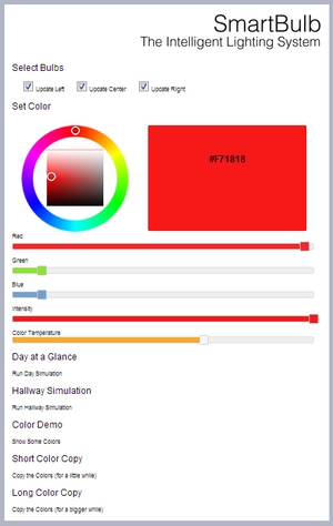
The web management interface is composed of a web front end and a message processing back end capable of transmitting the messages on the Digimesh wireless network.
Description of Functionality
The user makes adjustments to the interface. Changes are asynchronously transmitted for processing. The color values are processed to meet the requirements of the SmartBulbs and then encapsulated in a Google Protocol buffer message for transmission across the mesh network.
Design of Web Interface
The design of the web interface centered around using proven techniques to produce a reasonable interface. Since the project focus was on the lights and their applications the management interface was kept simple for purposes of economy as well as to keep presentation focus on the core components.
Front End
The front end was created from an end-user perspective to allow system control. The layout was designed to be compatible with non-multi-touch screens; meaning that the interface must fit comfortable on a single page, all elements must be large enough to activate without zooming, and all input must be usable with nothing more than a mouse. To meet this requirement the design included the use of HTML, CSS, jQuery, and jQuery UI. The plain and simple styling of jQuery UI were largely left alone with the exception of modifications to make the elements larger and more touch friendly. AJAX was selected as the method of transmitting data from the JavaScript interface to the server for processing. AJAX allows quicker response time without breaking the illusion of a full screen desktop application.
Back End
The backend must connect the web interface to the application. In this case this means making the crucial link between the communication layer and the user's input. Input is checked before being processed. The processed data is then passed to the communication layer.
Communication Layer
The communication layer is being treated separately from the back end. The communication layer forms the bridge between data processed on the web server to the SmartBulb mesh network. The communication layer must be compatible with the Google protocol buffers in use by the SmartBulb network. The communication layer also contains the functionality to send the data via a Digimesh wireless radio attached to the computer. One reason we choose to run the web server on Linux is because of how serial connections are treated under Linux -- they are treated just as text files. To send data via the wireless radio, the communication layer simply needs write to a file.
Implementation of Web Interface
Front End
The user interface was constructed using HTML and JavaScript. The jQuery JavaScript framework and the jQuery UI widgets were used extensively to produce an interactive interface capable of being driven through a touchscreen. Several design choices stemmed from the decision to make the interface touch based. The interface would be a single page without scrolling for easy touch navigation. The interface would also send all the data via AJAX to avoid the need to reload the page. A full screen browsing mode when coupled with AJAX allows a seamless interface that is quickly editable. HTML and CSS were used to create the structure and style of the web page. Color choice and demonstration modes when activated would send RGB color data to the message processing back end for asynchronous processing.
The following JavaScript shows how jQuery provides easy to use AJAX functionality. This snippet allows the data provided to be POSTed to a URL. The response from the server is caught and returned to a callback. In this example the callback simply provides a log to the console. Logging to the JavaScript console is crucial to accurate debugging of asynchronous tasks. As the tasks complete the data (and any errors) are conveniently printed.
$.ajax({
  type: "POST",
  url: "some.php",
  data: { name: "John", location: "Boston" }
}).done(function( msg ) {
  console.log( "Data Saved: " + msg );
});
To avoid flooding the mesh network AJAX calls to the message processor were rate limited using Underscore.js. Underscore.js is a JavaScript library that provides many convenient functions, one of which provides rate limiting functionality. To add a rate limit to an existing function
var throttled = _.throttle(function(){
  console.log("User Scrolled");
}, 100);
$(window).scroll(throttled);
Back End
Implementing the back end was relatively straightforward. The design requirements were clear: data must be received from an AJAX call, processed, and forwarded to the communication layer. A single PHP file acted as the data receiver and was the destination of the AJAX calls. The data receiver includes a function library created to provide data processing routines. These routines process the data from user input into the format required by the bulb.
Communication Layer
The communication layer was built using DrSlump's Protobuf-PHP library. The library is easy to use, once the protoc compiler is configured. Although we did not extensively test the functionality we believe that DrSlump's library does not properly encode message types. This flaw is easy to work around and should not count against the library so much as just be made aware of.
Implementation
This section includes implementation, but again, not the details, just the high level. For example, you can list the steps it takes to communicate over a sensor, or the steps needed to write a page of memory onto SPI Flash. You can include sub-sections for each of your component implementation.
Testing & Technical Challenges
Describe the challenges of your project. What advise would you give yourself or someone else if your project can be started from scratch again? Make a smooth transition to testing section and described what it took to test your project.
Custom Printed Circuit Board
In order to fulfill our system requirements, we opted to design our own custom printed circuit board (PCB). We ran into several challenges on the path to accomplishing this task:
- Software: We used Altium as our PCB CAD software, it's a sophisticated tool which allowed us to accomplish our task, but we had to put in several hours to learn the intricacies of the tool
- One critical error we ran into for our first iteration of the PCB is we did not know how to run the design rule check, and we had to manually correct them when the PCB arrived
- Altium was not set up to be used with multiple users with files syncing on Dropbox, so we ran into some trouble where changes weren't being executed properly
- Assembly: Due to cost constraints, we had to assemble the boards ourselves including the 100 pin microprocessor chip
- A few of our parts were quite delicate and required extra care to solder onto the board
- We made some mistakes which required de-soldering/rework
- Testing: We had to verify that our boards worked
- During programming some errors would result from shorts on the board
Our solutions:
- Software: We put in many hours to learn Altium, each team member irrespective of their expertise learned how to use Altium to an extent in order to assist with PCB related tasks
- After we ran into the ground errors on our first board, we were vigilant about design rule checking our design to make sure that rules and specifications were followed on our final iteration of the PCB
- In order to make sure our files were not subject to unwanted changes, we made sure to properly close the files and communicated with each other about the status of the project file. We also uploaded major milestone design changes to our repository
- Assembly: We utilized our own soldering expertise, improved our techniques, and learned new techniques to accomplish our board assembly
- For the 100 pin processor chip, Phil skillfully adapted the drag-solder technique, so he was solely in charge of processor chip soldering
- After making mistakes, we would review our work to avoid making the same mistake
- Testing: We would put on the minimum parts needed to test the processor and JTAG connection before moving onto the other parts
- To find shorts, we would use a multimeter to perform a continuity test and verification on the pins. We would also look at the processor chip (it was prone to shorts from the solder drag) under a magnifying glass/microscope
- Board shorting was a particularly difficult challenge we faced, and we would suggest very carefully assembling the board and paying attention to the components which are difficult to solder -- it costed us a lot of time and frustration when a hardware problem was confused with a software issue
Conclusion
Conclude your project here. You can recap your testing and problems. You should address the "so what" part here to indicate what you ultimately learnt from this project. How has this project increased your knowledge?
Project Video
Upload a video of your project and post the link here.
Project Source Code
Due to patent pending the source code is not listed for this project.
References
Acknowledgement
Any acknowledgement that you may wish to provide can be included here.
References Used
List any references used in project.
Appendix
You can list the references you used.
