Difference between revisions of "F15: Doorknock over Bluetooth"
Proj user20 (talk | contribs) (→Hardware Design) |
Proj user20 (talk | contribs) (→Hardware Design) |
||
| Line 90: | Line 90: | ||
=== Hardware Design === | === Hardware Design === | ||
Discuss your hardware design here. Show detailed schematics, and the interface here. | Discuss your hardware design here. Show detailed schematics, and the interface here. | ||
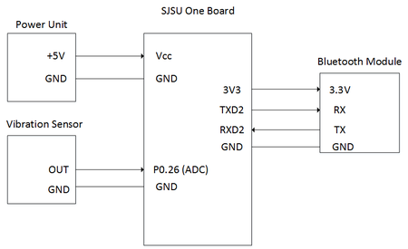
| − | [[File:cmpe146_F15_Doorknock_HWSchematic.png|thumb | + | [[File:cmpe146_F15_Doorknock_HWSchematic.png|thumb|450px|Figure 1. Hardware Design Schematic]] |
| + | For the Bluetooth module, UART communication was used to send data to the mobile application, alerting the user of a knock on the door. | ||
| + | As shown in Figure 1, the ADC input pin (P0.26) of the SJSU One Board was used to collect the analog signal transmitted by the Piezo vibration sensor. Once the analog signal is collected, it would be converted to a digital value using analog-to-digital conversion methods built into the board. This value would then be measured to determine if the vibration was significant enough to be a knock on the door. | ||
| + | |||
| + | The RXD2 and TXD2 pins on the CPU were used for UART communication with the Bluetooth module. Once a knock was detected by the vibration sensor, a single data byte would be transmitted from the controller to the HC-06 which would be able to transmit the data over Bluetooth to the paired mobile device. | ||
| + | |||
| + | In summary, the pin functionality is briefly described below: | ||
| + | *P0.26 is configured to be the ADC input from the vibration sensor. | ||
| + | *TXD2 is to send data using the UART2 communication bus to the Bluetooth module. | ||
| + | *RXD2 is to receive data using the UART2 communication bus from the Bluetooth module. | ||
Revision as of 06:23, 10 December 2015
Contents
Grading Criteria
- How well is Software & Hardware Design described?
- How well can this report be used to reproduce this project?
- Code Quality
- Overall Report Quality:
- Software Block Diagrams
- Hardware Block Diagrams
- Schematic Quality
- Quality of technical challenges and solutions adopted.
Project Title
Doorknock over Bluetooth
Abstract
This project is to build a door knock sensor that is mounted on a user's door. Using a vibration sensor, the device will alert the user when someone knocks at their door by sending a notification over Bluetooth to the user's mobile android application, that will be developed to pair with the device.
Objectives & Introduction
Show list of your objectives. This section includes the high level details of your project. You can write about the various sensors or peripherals you used to get your project completed.
Team Members & Responsibilities
- Andrew Herbst
- Sensor interface and UART communication
- Banks Lin
- Android developer and bluetooth communication
Schedule
Show a simple table or figures that show your scheduled as planned before you started working on the project. Then in another table column, write down the actual schedule so that readers can see the planned vs. actual goals. The point of the schedule is for readers to assess how to pace themselves if they are doing a similar project.
| Week# | Date | Task | Status |
|---|---|---|---|
| 1 | 10/23 | Complete Abstract | Completed |
| 2 | 10/30 | Further develop wiki page and purchase/receive components | In Progress |
| 3 | 11/6 | Complete bluetooth and Android communication | In Progress |
| 4 | 11/13 | Have basic response from the sensor | In Progress |
| 5 | 11/20 | Actual communication with bluetooth module | In Progress |
| 6 | 11/27 | Debugging on Android side | In Progress |
| 7 | 12/4 | Finish last debugging and construct hardware | In Progress |
Parts List & Cost
Give a simple list of the cost of your project broken down by components. Do not write long stories here.
- Piezo Element (vibration sensor): $1.50
- JBtek HC-06 Bluetooth Module: $8
- LPC1758 SJ One Board: $80
- Motorola Nexus 6: $600
Total Cost: $689.50
Design & Implementation
The design section can go over your hardware and software design. Organize this section using sub-sections that go over your design and implementation.
Hardware Design
Discuss your hardware design here. Show detailed schematics, and the interface here.
For the Bluetooth module, UART communication was used to send data to the mobile application, alerting the user of a knock on the door.
As shown in Figure 1, the ADC input pin (P0.26) of the SJSU One Board was used to collect the analog signal transmitted by the Piezo vibration sensor. Once the analog signal is collected, it would be converted to a digital value using analog-to-digital conversion methods built into the board. This value would then be measured to determine if the vibration was significant enough to be a knock on the door.
The RXD2 and TXD2 pins on the CPU were used for UART communication with the Bluetooth module. Once a knock was detected by the vibration sensor, a single data byte would be transmitted from the controller to the HC-06 which would be able to transmit the data over Bluetooth to the paired mobile device.
In summary, the pin functionality is briefly described below:
- P0.26 is configured to be the ADC input from the vibration sensor.
- TXD2 is to send data using the UART2 communication bus to the Bluetooth module.
- RXD2 is to receive data using the UART2 communication bus from the Bluetooth module.
Power Unit:
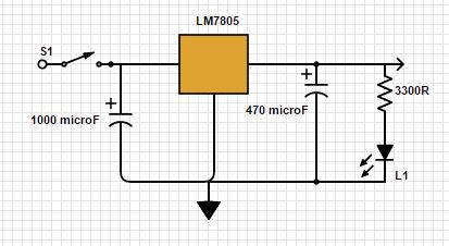
A 9V battery was used to power the device. However, a voltage regulator was designed to supply a 5V output to the SJSU One board.
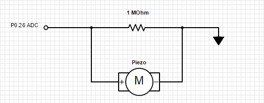
Vibration Sensor: The device was equipped with a Piezo Vibration sensor to detect the knock. EXPLAIN HOW IT WORKS. When a vibration is detected, an analog signal is sent to the microcontroller.
Bluetooth Module:
The JBtek HC-06 Bluetooth module was chosen for this device because it is a widely-used device and is compatible with the Android Phone.
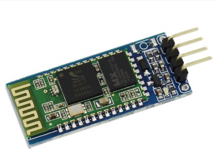 Image obtained from: http://ecx.images-amazon.com/images/I/61F4XCwfXEL._SX425_.jpg (add to image description)
Hardware Interface
In this section, you can describe how your hardware communicates, such as which BUSes used. You can discuss your driver implementation here, such that the Software Design section is isolated to talk about high level workings rather than inner working of your project.
Software Design
Show your software design. For example, if you are designing an MP3 Player, show the tasks that you are using, and what they are doing at a high level. Do not show the details of the code. For example, do not show exact code, but you may show psuedocode and fragments of code. Keep in mind that you are showing DESIGN of your software, not the inner workings of it.
Bluetooth Task
Sensor Task
Implementation
This section includes implementation, but again, not the details, just the high level. For example, you can list the steps it takes to communicate over a sensor, or the steps needed to write a page of memory onto SPI Flash. You can include sub-sections for each of your component implementation.
Testing & Technical Challenges
Describe the challenges of your project. What advise would you give yourself or someone else if your project can be started from scratch again? Make a smooth transition to testing section and described what it took to test your project.
Include sub-sections that list out a problem and solution, such as:
My Issue #1
Discuss the issue and resolution.
Conclusion
Conclude your project here. You can recap your testing and problems. You should address the "so what" part here to indicate what you ultimately learnt from this project. How has this project increased your knowledge?
Project Video
Upload a video of your project and post the link here.
Project Source Code
References
Acknowledgement
Any acknowledgement that you may wish to provide can be included here.
References Used
List any references used in project.
Appendix
You can list the references you used.
