Difference between revisions of "S15: CAN controlled RGB LED cubes"
Proj user12 (talk | contribs) (→Two nodes CAN configuration) |
(→Grading Criteria) |
||
| (216 intermediate revisions by one other user not shown) | |||
| Line 1: | Line 1: | ||
| − | |||
| − | |||
| − | |||
| − | |||
| − | |||
| − | |||
| − | |||
| − | |||
| − | |||
| − | |||
| − | |||
| − | |||
== Project Title == | == Project Title == | ||
CAN controlled RGB LED cubes | CAN controlled RGB LED cubes | ||
| − | |||
== Abstract == | == Abstract == | ||
| − | In this project, data( | + | In this project, data(8 byte or less) sent from an android application will be displayed in a 3D form on a LED cube. Two LED cubes will be connected to two different SJone boards, these SJone boards are connected to a third SJone board using CAN bus. One LED board will be displaying some patters based upon the input from User and other LED cube will display characters one by one. The LED cubes will be connected to their respective SJ |
| − | different SJone boards, these SJone boards are connected to a third SJone board using CAN bus. The LED cubes will be connected to their respective SJ | ||
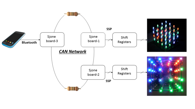
boards through shift registers. The boards will implement SSP protocol to communicate with the shift registers. A bluetooth module is connected to third | boards through shift registers. The boards will implement SSP protocol to communicate with the shift registers. A bluetooth module is connected to third | ||
| − | SJone board. | + | SJone board. Android application sends data to be displayed along with the information about the SJone board(one of the LED cube) to be selected. |
| − | Android application sends data to be displayed along with the information about the SJone board(one of the LED cube) to be selected. | ||
| − | [[File: | + | [[File:S15_244_G19_IMG_1.png|650px|thumb|centre|Fig. 1: Project Block Diagram]] |
== Objectives & Introduction == | == Objectives & Introduction == | ||
| − | + | The main objective is to understand and implement CAN bus interface between 3 nodes. CAN Master node sends data with specific message id and Slave Nodes listen to their message id's and reads the data from CAN bus. | |
| + | The Secondary objective was to design two LED cubes and transmit data to LED cube via SSP interface. | ||
| + | * In our project, we used Timer Interrupts, UART Interrupts, SSP and CAN interface. | ||
| + | |||
=== Team Members & Responsibilities === | === Team Members & Responsibilities === | ||
| Line 45: | Line 33: | ||
* '''Daamanmeet Paul''' | * '''Daamanmeet Paul''' | ||
** Android application development | ** Android application development | ||
| − | |||
== Schedule == | == Schedule == | ||
| − | + | ||
{| class="wikitable" | {| class="wikitable" | ||
| Line 107: | Line 94: | ||
-Interfacing of LED cubes with shift registers | -Interfacing of LED cubes with shift registers | ||
| − | | | + | | Completed |
| 4/26 | | 4/26 | ||
|- | |- | ||
| Line 119: | Line 106: | ||
-Initially making two-nodes CAN configuration(Completed) | -Initially making two-nodes CAN configuration(Completed) | ||
| − | -Three nodes CAN configuration( | + | -Three nodes CAN configuration(Completed) |
| Completed | | Completed | ||
| 4/30 | | 4/30 | ||
| Line 127: | Line 114: | ||
| Generating patterns on LED cubes | | Generating patterns on LED cubes | ||
-Building libraries for generating Alphabets & numbers on the LED cubes | -Building libraries for generating Alphabets & numbers on the LED cubes | ||
| − | | | + | | Completed |
| 5/7 | | 5/7 | ||
|- | |- | ||
| Line 134: | Line 121: | ||
| Implementing FreeRTOS for the system | | Implementing FreeRTOS for the system | ||
-Implementing queue RTOS feature to connect the bluetooth interface and the CAN interface of the LPC1758 board | -Implementing queue RTOS feature to connect the bluetooth interface and the CAN interface of the LPC1758 board | ||
| − | | | + | | Completed |
| 5/10 | | 5/10 | ||
|- | |- | ||
| Line 140: | Line 127: | ||
| 5/10 | | 5/10 | ||
| Final Debugging & testing | | Final Debugging & testing | ||
| − | | | + | | Completed |
| 5/15 | | 5/15 | ||
|} | |} | ||
| Line 193: | Line 180: | ||
|- | |- | ||
! scope="row"| 9 | ! scope="row"| 9 | ||
| − | | ULN | + | | ULN 2003A |
| − | | | + | | 6 |
| − | | | + | | 2 |
|- | |- | ||
|} | |} | ||
== Design & Implementation == | == Design & Implementation == | ||
| − | |||
| + | === Hardware Design & Interface === | ||
| + | In our project, we are using CAN bus, LED cude interface with SPI using shift registers, Bluetooth interface with UART2. All of these interfaces are described below in detail. | ||
| + | |||
| + | === LED Cube interface with SJ-One Board === | ||
| + | |||
| + | |||
| + | *Shift registers have been used to communicate between the SJone board and the LED cubes. As the dimension of the cue is 4 x 4 x 4, it needs a total of 28 pins to control it, 16 pins to control 16 groups of 4 LED anodes and 12 pins to control 4 planes of the RGB lines. As we do not have that many pins on SJone board, we will be using 4 Serial- input-parallel-output shift registers to drive the LED terminals. This eases our job as only 5 pins are used from the board to drive 28 LED terminals. \ | ||
| + | {| | ||
| + | |[[File:S15_244_G19_IMG_2.png|300px|thumb|left|Fig. 2: SC74HC595 Shift Register Pin Diagram]] | ||
| + | |[[File:SC74HC595 Internal Architecture.png|400px|thumb|right|Fig. 3: Shift Register Timing Diagram]] | ||
| + | |} | ||
| − | + | *The communication bus used between the LPC1758 board and the shift registers is SSP-Synchronous Serial Port. The driver written for the communication is as shown in Fig.All the shift registers are cascaded, meaning the serial output of one, connected to the serial input of the other. This way a total of 32 bits of serial data from the board can be converted into parallel outouts which are given to its respective LED terminals. | |
| − | |||
| + | *'''Shift Register pin connections with the board:''' | ||
| + | We are using 8 bits from the shift register as parallel output data,VCC and ground connections are made with the board.The SRCLK is bit shifting clock which comes from the SSP1 clock.The SRCLR is an active low pin and is being driven high along with the Output Enable permanently to never reset the storage register in the shift register and to enable the shift register respectively. RCLK is the latching clock and It is connected with a GPIO pin on the board. When this pin is low the output of the shift register is in the floating state, no matter where the bit is reached in the storage register. When this pin becomes high, the storage register data latches with the output pins. The SER is the serial input data which comes from the board as the MOSI input. The OUT pin is the output serial data. This is the same incoming data into the register. But, it has been shifted 8 times first and then only given out and it is used for cascading. | ||
| + | {| | ||
| + | |[[File:S15_244_G19_IMG_4.png|400px|thumb|left|Fig. 4: 3x3x2 Cube Test)]] | ||
| + | |[[File:S15_244_G19_IMG_5_Shift register cascading.png|600px|thumb|right|Fig. 5: Shift Register Cascading Logic]] | ||
| + | |} | ||
| − | + | *'''Cascading of the Shift Register and its testing:''' | |
| − | In this | + | A sample LED cube of dimension 3x3x2 was made in order to plan for the delicate construction of the actual LED cubes. This sample cube was interfaced with 3 cascaded shift register. This was simply done by connecting the serial output pin of 1st register with serial input pin of the second one. After one clock a bit output of a shift register shifts to the immediate next bit output of the register. In this way as shown in the figure, after 16 clock cycles a total of two bytes can be represented parallely at the shift register output. Note - In SPI communication the MSB of the byte always goes first. |
| − | + | {| | |
| − | + | |[[File:S15_244_G19_IMG_6.png|400px|thumb|left|Fig. 6: Cube's Anode & Plane Naming Convention]] | |
| − | + | |[[File:S15_244_G19_IMG_7.png|700px|thumb|right|Fig. 7: LED Cubes's Circuit Design]] | |
| − | + | |} | |
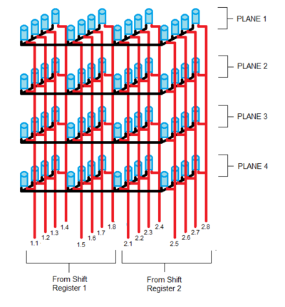
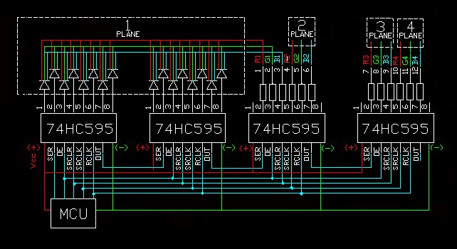
| − | The | + | *'''Cube's naming conventions & working logic:''' |
| − | + | So after the testing was successful, an actual LED cube was constructed with the pin and plane naming conventions as shown in the diagram above. a single plane of 16 LEDs have 1 common connection for Red, 1 common connection for Green, 1 common connection for Blue. The planes are horizontally constructed and the anodes are vertically connected. A single vertical line of anodes requires 1 pin. Likewise, there are a total of 16 anode line connections. In the circuit diagram, the shift registers has the SRCLR and OE, permanently pulled high for enabling the logic. The SRCLK and the RCLK are also commonly connected to the other shift registers SRCLK and RCLK pins respectively. Now, the RCLK is used to latch the data to the output pins. We do not want the data to appear at the output just when we are shifting the bits. Otherwise, | |
| − | + | due to the perception of vision, we will see some garbage output. Hence, just when we are done shifting a total of 32 output bit (4 bytes), we will latch the data to the output pins by pulling the RCLK pin high using software(GPIO) and then again lowering it later. | |
| − | [[File: | + | {| |
| − | [[File: | + | |[[File:S15_244_G19_IMG_8.png|550px|thumb|left|Fig. 8: Final LED Cube's Top View]] |
| + | |[[File:S15_244_G19_IMG_9.png|490px|thumb|right|Fig. 9: Printed Alphabet 'N' from Side View]] | ||
| + | |} | ||
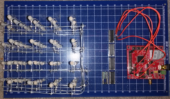
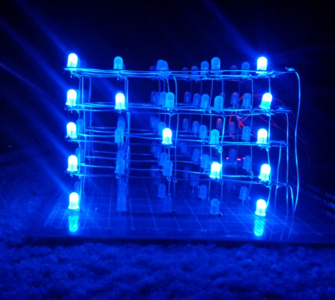
| + | *'''Final Hardware and its testing:''' | ||
| + | One LED cube was made of dimension 4x4x4 that can display any color and another cube was made of dimension 5x5x4 (Blue) to display the letters more accurately. To turn ON and led ,only that particular anode line should be given logic 1 by the shift registers and every other anode line should be given logic 0. At the cathode side, only that particular planes, cathode must be pulled low and every other cathode lines high. This will apply a forward voltage across the LED and it will glow. In case of multicolor LED cube, a particular cathode should be selected to turn ON a specific color. Every color can be made using RGB. So as to make a color, a combination of RGB can be used. This can be achieved by giving red color to an LED for some specific time, then blue color for some time and then green color for some time. This way, due to very high frequency of this switching, human eyes would not see three different colors, but one color which is a mixture of these three colors. The resultant color depends on the right mix of the RGB colors. If we want to see orange color, we will have to incresing the delay time of the Red color first and then increase the Yellow color in equal proportion. Blue is not needed here. VOILA! we have an orange color LED. In the above diagram, a letter N is shown on the cube. It seems that each LED of this 'N' is glowing at the same time, while it truely is not. Only one plane of LEDs is working at once. This is the magic of 'perception of vision'. | ||
| − | ==Two nodes CAN configuration== | + | === Two nodes CAN configuration === |
Hardware setup | Hardware setup | ||
| − | * The below diagram is for Two nodes CAN configuration. CAN1 is used on SJBoard with CAN transceiver MCP 2551. The interfacing with MCP2551 and SJBoard is shown with the pin diagram. This setup is for communication between two SJBoards using CAN protocol. Here, Termination resisters value between CANH and CANL is 120 Ohms. The RS pin is used to select High-speed, Slope-control or Standby modes via an external biasing resistor | + | * The below diagram is for Two nodes CAN configuration. CAN1 is used on SJBoard with CAN transceiver MCP 2551. The interfacing with MCP2551 and SJBoard is shown below with the pin diagram. This setup is for communication between two SJBoards using CAN protocol. Here, Termination resisters value between CANH and CANL is 120 Ohms. The RS pin is used to select High-speed, Slope-control or Standby modes via an external biasing resistor and is connected to the ground directly. External 5V power supplier is used to power up both MCP 2551 CAN transceiver ICs. P0.0 and P0.1 on SJBoard are for RXD1 and TXD1 respectively for CAN1. |
| − | + | ||
| − | * In this configuration | + | * This below 2 nodes CAN configuration is for the testing of the CAN protocol. In this project, 3 nodes CAN configuration is used. Third CAN node can be inserted to this network easily. CANH of the third node is connected to the CANH channel of the network and CANL is connected to CANL channel of netwrork. |
| + | |||
| + | |||
| + | [[File:S15_244_G19_IMG_10.png|700px|thumb|center|Fig. 10: CAN Implementation Between The Boards]] | ||
| + | |||
| + | === Bluetooth module Interface === | ||
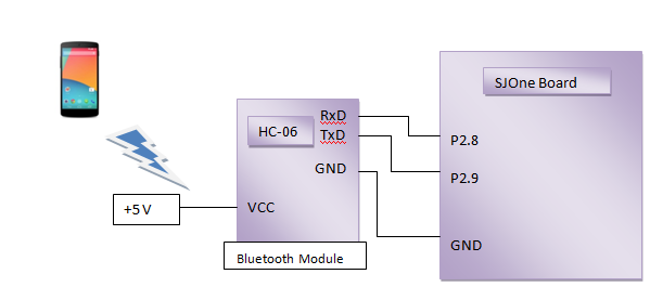
| + | *Data from Android application is sent over Bluetooth to 'Bluetooth receiver (HC-06)'. Bluetooth receiver is connected to UART 2 as per below diagram. | ||
| + | * Bluetooth module is connected with UART2 on SJSU-One board. HC-06 needs 5V, which is being provided externally. Tx Pin of HC-06 is connected with P2.9 (Rx of Uart2), Rx pin is connected with P2.8 of Sjsu-One board, GND is made common and Vcc is connected with 3.3V (took from SJSU one board). Below is the pin diagram from Bluetooth-Uart connections. | ||
| + | |||
| + | [[File:S15_244_G19_IMG_11.png|600px|thumb|center|Fig. 11: Bluetooth Connectivity Between SJone Board And Cell Phone]] | ||
| − | + | == Software Design == | |
| − | === | + | === SSP Communication === |
| − | + | int buffer(char out1, char out2,char out3,char out4) | |
| + | {while(!(LPC_SSP1->SR & 0x2)); | ||
| + | LPC_SSP1->DR = out1; // sending a total of 4 bytes for 4 shift registers | ||
| + | while(!(LPC_SSP1->SR & (1<<4))); // waiting for a byte to be sent succesfully | ||
| + | LPC_SSP1->DR = out2; | ||
| + | while(!(LPC_SSP1->SR & (1<<4))); | ||
| + | LPC_SSP1->DR = out3; | ||
| + | while(!(LPC_SSP1->SR & (1<<4))); | ||
| + | LPC_SSP1->DR = out4; | ||
| + | while(!(LPC_SSP1->SR & (1<<4))); | ||
| + | LPC_GPIO0->FIOSET = (1<<1); // setting the storage register clock pin high after sending 32 bits so | ||
| + | delay_us(1); // that the it latches the shift register output to the output pins | ||
| + | LPC_GPIO0->FIOCLR = (1<<1); | ||
| + | while(!(LPC_SSP1->SR & 0x4)); | ||
| + | return LPC_SSP1->DR; | ||
| + | } | ||
| + | === CAN Communication === | ||
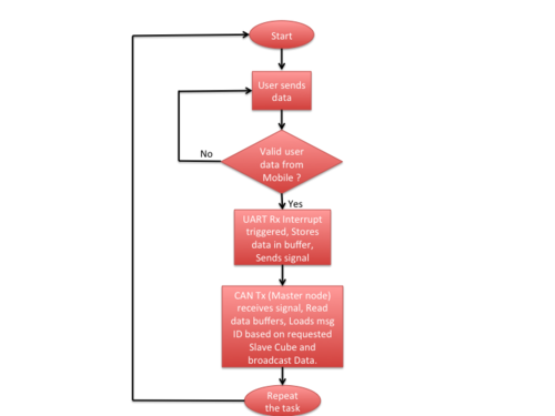
| + | * A task is created for CAN transmission at transmission side and this task checks for the signal from the UART Interrupt handler; on receiving the signal, data on a requested board will be sent using CAN protocol. | ||
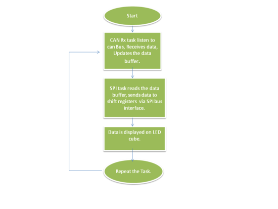
| + | * Receiver side listens only to the messages from specific message id and on receiving the message, it updates the data buffer. | ||
| + | === Bluetooth module Interface === | ||
| + | *'''Protocol used to send data from application''': 8-byte data (or less ) send over Bluetooth will be displayed on the one of the LED cubes. If we need to display characters ‘SJSU’ on LED cube connected to Sj-One board 1. Then user should transmit < 1SJSU$>; where first field is board on which data is to be displayed followed by words to display, ‘$’ sign is must be added at the end to indicate the end of string(data). If the data to be displayed is 8 bytes long, then ’$’ is not required. | ||
| + | *The first flied should be either 1 or 2 (to select from one of 2 LED cubes). | ||
| + | *In our project, we are using UART2 connection with Bluetooth module. Baud rate is set at 9600 bps.Once the data is sent over mobile to Bluetooth device, Receive interrupt will occur and interrupt handler will be called. Interrupt handler sends signal to respective task(CAN Transmitter task) and task which is waiting on signal then reads the FIFO. The first character read by task will be ‘board number’ followed by words to be printed and ‘$’ sign. On reading the whole message the task sends message to CAN transmitter to send data over CAN bus. | ||
| − | + | === Android Application Development === | |
'''Tools used to Develop Android Application:''' | '''Tools used to Develop Android Application:''' | ||
* Android Studio based on IntelliJ IDEA. | * Android Studio based on IntelliJ IDEA. | ||
| − | |||
* Java Development kit 7 by Oracle. | * Java Development kit 7 by Oracle. | ||
| − | |||
* Android ADB interface. | * Android ADB interface. | ||
| − | |||
| − | |||
'''Application Features:''' | '''Application Features:''' | ||
* Bluetooth pairing up to 6 devices at a time. | * Bluetooth pairing up to 6 devices at a time. | ||
| − | |||
* Facility to change Transmission Protocol within the Application. | * Facility to change Transmission Protocol within the Application. | ||
| − | |||
* Send Data serially to any serial Bluetooth Device. | * Send Data serially to any serial Bluetooth Device. | ||
| − | |||
* Receive Data serially from any Bluetooth device using same protocol. | * Receive Data serially from any Bluetooth device using same protocol. | ||
| Line 264: | Line 294: | ||
http://bitfountain.io/courses/mini-android | http://bitfountain.io/courses/mini-android | ||
| − | '''Bluetooth | + | '''Bluetooth API setup :''' |
* BluetoothAdapter | * BluetoothAdapter | ||
| − | |||
Used for the local Bluetooth adapter (Bluetooth radio). The BluetoothAdapter is the entry-point for all Bluetooth interaction. It is used to discover other Bluetooth devices, query a list of bonded (paired) devices, instantiate a BluetoothDevice using a known MAC address, and create a BluetoothServerSocket to listen for communications from other devices. | Used for the local Bluetooth adapter (Bluetooth radio). The BluetoothAdapter is the entry-point for all Bluetooth interaction. It is used to discover other Bluetooth devices, query a list of bonded (paired) devices, instantiate a BluetoothDevice using a known MAC address, and create a BluetoothServerSocket to listen for communications from other devices. | ||
| + | * Connecting Bluetooth devices. | ||
| − | Android | + | The Android has the Sjsu board connected Bluetooth module stored in a BluetoothDevice object. The next objective is to form the connection between the Android and the Sjsu Board. This work should take place in separate thread. Source Code of the application is provided under Android_application folder in the sourceforge link. |
| − | |||
| − | |||
| − | |||
| − | |||
| − | |||
| − | |||
| − | |||
| − | |||
| − | |||
| − | |||
| − | |||
| − | |||
| − | |||
| − | |||
| + | *'''Application BlueT19 GUI''' | ||
| − | + | * Application Home Screen | |
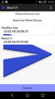
| − | + | In this screen, the first button (Search for the paired devices) is used to search for the paired Bluetooth devices which are already paired with the device and from this list of devices we can choose whichever device to communicate data. Then, the second button located in the bottom is used to finally establish the connection. If the device you are selecting is not a serial data compatible then an error message is also generated. Figure is shown below. | |
| − | |||
| − | + | [[File:S15_244_G19_IMG_12.png]] | |
| − | |||
| − | |||
| − | |||
| − | |||
| − | + | * Application Main Screen | |
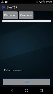
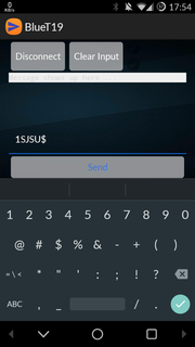
| − | + | In this screen, there are two options provided that are we can send and receive serial data simultaneously. In the upper part of the screen the buttons are provided to disconnect with the device and clear the input received from the other connected device. The serial data received is displayed right under the above two button. In the lower part the screen, we have the option of sending serial data to the connected device. We can directly enter data by clicking Enter Command screen option by using onscreen keyboard. After entering the desired data we can send it by clicking the Send button. If user Input anything invalid other then suggested transmission protocol standard, then an error message will be returned back to Android application in received message section and no change in output will occur at the output LED cubes. | |
| − | |||
| − | + | [[File:S15_244_G19_IMG_13.png]] [[File:S15_244_G19_IMG_14.png]] | |
| − | |||
| − | |||
| − | |||
| − | |||
| − | |||
| − | |||
| − | |||
| − | |||
| − | |||
| − | |||
| − | |||
| − | |||
| − | |||
| − | |||
| − | |||
| − | |||
=== Implementation === | === Implementation === | ||
| − | + | Below are the flow charts for 'Data' transfer from 'Android Device' via CAN bus to 'LED Cube'. | |
| + | {| | ||
| + | |[[File: S15_244_G19_IMG_15.png|500px|thumb|left|Transmitter Flow Chart]] | ||
| + | |[[File: S15_244_G19_IMG_16.png|550px|thumb|right| Receiver Flow Chart]] | ||
| + | |} | ||
== Testing & Technical Challenges == | == Testing & Technical Challenges == | ||
| − | + | === My Issue #0 === | |
| − | + | *Due to connection of Rs pin of CAN transceiver to ground via 1K resistor, CAN transmission was not working. So after directly connecting this pin to ground we resolved this issue. | |
| − | + | === My Issue #1 === | |
| + | *Sending a long string of data from Application: This issue was mainly because we were not using Interrupts hence FIFO was overflowing which results into loss of data. | ||
| + | *Getting garbage value during read from UART2: This was because of baud rate, on using baud rate 9600 with precision ±3 %, this issue got resolved. | ||
| + | * As we need to send data from android application in a particular format say '1SJSU$',there were several loop holes in this, what if user sends '1hello' and how board should understand, to solve several loop holes, we used Timer Interrupts. Now User can send in two parts such as '1SJS' and 'U$', but should be sent within 3 seconds. | ||
| − | === My Issue # | + | === My Issue #2 === |
| − | + | *While generating patterns on LED cubes, we were getting problem of different intensity of LEDs on same LED cube. To resolve this problem we removed IC- ULM 2003 and we connected the cathodes of LED to shift register via resistors instead of using ULN. | |
| + | *Also, we used 22 ohm resistor according to the electrical characteristics, but we found out prcatically, that even a 10 ohm resistor will work. The 10 ohm resistor is properly sinking the cathode current and also we are getting optimal brightness of the LEDS. | ||
| + | *Also due to loose soldering, patterns were not getting generated, but this was solved quickly with the help of a multimeter. | ||
| + | *Because of the clock signal given to many shift registers at once, the capacitance of the line decreased, hence we needed to find a particular SPI frequency. | ||
== Conclusion == | == Conclusion == | ||
| − | + | ||
| + | Altogether, we really enjoyed being in this class and do this project. We faced many difficulties throughout the semester including searching for the project, planning and executing it. But each time we faced a problem, we got to learn many new things. The difficulties led to the deeper knowledge. All of us were stucked at our individual tasks at some point or the other, but we helped each other and finally made our project up and running. Not to mention, Preet was always easily approachable. Our project is running from top to bottom, sending an alphabet or a number from a cell phone, passing it to other board on the CAN network and printing on the LED cubes. The character is sent to only that node for which it was meant for. There are also patterns of the display in the cubes which really looks beautiful. In case if an a user uses wrong format to send a message from android phone, a message will be sent from LPC board over bluetooth to mobile device about the error. We have uploaded everything regarding this project on this page. We honestly appreciate your interest in reading this page. Thank you! | ||
=== Project Video === | === Project Video === | ||
| − | + | https://www.youtube.com/watch?v=RFz86Flb9JA | |
=== Project Source Code === | === Project Source Code === | ||
| Line 350: | Line 356: | ||
== References == | == References == | ||
=== Acknowledgement === | === Acknowledgement === | ||
| − | + | We would like to thank Preet for teaching the concepts in a very practical sense in the class. It really helped us in the implementation of the project. We would also like to thank Shashank who was always ready to help and who also gave many ideas of what we can do in the project. | |
=== References Used === | === References Used === | ||
| − | + | *Preetpal Kang's lecture notes of CMPE 244, Computer Engineering, San Jose State University, Jan-May 2015. | |
| + | *http://www.nxp.com/documents/user_manual/UM10360.pdf | ||
| + | *http://gemlit.com/howto/ | ||
| + | *http://www.nxp.com/documents/data_sheet/74HC_HCT595.pdf | ||
| + | *http://www.ti.com/lit/ds/symlink/uln2003a.pdf | ||
| + | *http://www.keil.com/download/docs/385.asp | ||
| + | *http://www.keil.com/forum/19707/uart-interrupt/ | ||
=== Appendix === | === Appendix === | ||
You can list the references you used. | You can list the references you used. | ||
Latest revision as of 15:58, 27 May 2015
Contents
Project Title
CAN controlled RGB LED cubes
Abstract
In this project, data(8 byte or less) sent from an android application will be displayed in a 3D form on a LED cube. Two LED cubes will be connected to two different SJone boards, these SJone boards are connected to a third SJone board using CAN bus. One LED board will be displaying some patters based upon the input from User and other LED cube will display characters one by one. The LED cubes will be connected to their respective SJ boards through shift registers. The boards will implement SSP protocol to communicate with the shift registers. A bluetooth module is connected to third SJone board. Android application sends data to be displayed along with the information about the SJone board(one of the LED cube) to be selected.
Objectives & Introduction
The main objective is to understand and implement CAN bus interface between 3 nodes. CAN Master node sends data with specific message id and Slave Nodes listen to their message id's and reads the data from CAN bus. The Secondary objective was to design two LED cubes and transmit data to LED cube via SSP interface.
- In our project, we used Timer Interrupts, UART Interrupts, SSP and CAN interface.
Team Members & Responsibilities
- Chitrang Talaviya
- LED cube design
- Implementing CAN protocol
- Bluetooth module interfacing
- Navjot Singh
- Implementing CAN protocol
- Bluetooth module interfacing
- FreeRTOS environment
- Anuj Korat
- LED cube design
- Generating dynamic patterns
- Implementing SSP with the shift registers
- Daamanmeet Paul
- Android application development
Schedule
| Week# | Start Date | Task | Status | Completion Date |
|---|---|---|---|---|
| 1 | 3/15 | Finalizing & ordering components
-Going through the requirements of the project -Order hardware components based on the final list |
Completed | 3/17 |
| 2 | 3/27 | 3x3x2 LED cube testing with SPI interfacing
-Studying the SC74HC595 shift register datasheet -Constructing a 3x3x2 LED cube for testing purpose -Interfacing of shift register using SSP1 with LPC1758 -Cascading of 4 shift registers using SSP1 to control anodes & RGB cathodes |
Completed | 4/10 |
| 3 | 4/8 | Bluetooth Interface with SJone board through Android APK
-Testing the AT commands of Bluetooth HS-06 V1.06 module using hyperterminal(Completed) -Testing interfacing of bluetooth using UART2(Completed) |
Completed | 4/17 |
| 4 | 4/8 | Android application
-Communication between bluetooth module and an android application(Completed) |
Completed | 4/25 |
| 5 | 4/16 | 4x4x4 LED cube construction
-Building 2 LED cubes -Interfacing & cascading of the shift registers with SJone boards to control 16 anodes and 12 cathodes using SIPO configuration of shift register -Interfacing of LED cubes with shift registers |
Completed | 4/26 |
| 6 | 4/20 | CAN protocol programming
-Studying the CAN protocol datasheet(Completed) -Setting up the interface of CAN transceiver and SJone boards(Completed) -Initially making two-nodes CAN configuration(Completed) -Three nodes CAN configuration(Completed) |
Completed | 4/30 |
| 7 | 4/27 | Generating patterns on LED cubes
-Building libraries for generating Alphabets & numbers on the LED cubes |
Completed | 5/7 |
| 8 | 5/1 | Implementing FreeRTOS for the system
-Implementing queue RTOS feature to connect the bluetooth interface and the CAN interface of the LPC1758 board |
Completed | 5/10 |
| 9 | 5/10 | Final Debugging & testing | Completed | 5/15 |
Parts List & Cost
| # | Components | Quantity | Price($)/component |
|---|---|---|---|
| 1 | RGB LEDs pack of 100 | 2 | 9.95 |
| 2 | CAN transceivers | 15 | Free |
| 3 | Shift registers, SC74HC595 | 10 | 1.49 |
| 4 | SJone boards | 3 | 80 |
| 5 | Bluetooth module | 1 | 20 |
| 6 | Steel wire | 1 | 8 |
| 7 | Soldering kit | 1 | ~40 |
| 8 | Jumper wires(each type) | 1 | 25 |
| 9 | ULN 2003A | 6 | 2 |
Design & Implementation
Hardware Design & Interface
In our project, we are using CAN bus, LED cude interface with SPI using shift registers, Bluetooth interface with UART2. All of these interfaces are described below in detail.
LED Cube interface with SJ-One Board
- Shift registers have been used to communicate between the SJone board and the LED cubes. As the dimension of the cue is 4 x 4 x 4, it needs a total of 28 pins to control it, 16 pins to control 16 groups of 4 LED anodes and 12 pins to control 4 planes of the RGB lines. As we do not have that many pins on SJone board, we will be using 4 Serial- input-parallel-output shift registers to drive the LED terminals. This eases our job as only 5 pins are used from the board to drive 28 LED terminals. \
- The communication bus used between the LPC1758 board and the shift registers is SSP-Synchronous Serial Port. The driver written for the communication is as shown in Fig.All the shift registers are cascaded, meaning the serial output of one, connected to the serial input of the other. This way a total of 32 bits of serial data from the board can be converted into parallel outouts which are given to its respective LED terminals.
- Shift Register pin connections with the board:
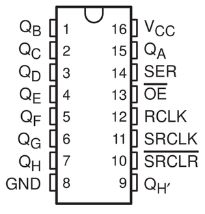
We are using 8 bits from the shift register as parallel output data,VCC and ground connections are made with the board.The SRCLK is bit shifting clock which comes from the SSP1 clock.The SRCLR is an active low pin and is being driven high along with the Output Enable permanently to never reset the storage register in the shift register and to enable the shift register respectively. RCLK is the latching clock and It is connected with a GPIO pin on the board. When this pin is low the output of the shift register is in the floating state, no matter where the bit is reached in the storage register. When this pin becomes high, the storage register data latches with the output pins. The SER is the serial input data which comes from the board as the MOSI input. The OUT pin is the output serial data. This is the same incoming data into the register. But, it has been shifted 8 times first and then only given out and it is used for cascading.
- Cascading of the Shift Register and its testing:
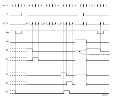
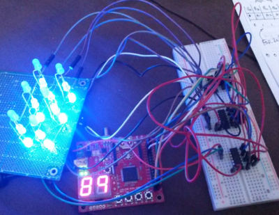
A sample LED cube of dimension 3x3x2 was made in order to plan for the delicate construction of the actual LED cubes. This sample cube was interfaced with 3 cascaded shift register. This was simply done by connecting the serial output pin of 1st register with serial input pin of the second one. After one clock a bit output of a shift register shifts to the immediate next bit output of the register. In this way as shown in the figure, after 16 clock cycles a total of two bytes can be represented parallely at the shift register output. Note - In SPI communication the MSB of the byte always goes first.
- Cube's naming conventions & working logic:
So after the testing was successful, an actual LED cube was constructed with the pin and plane naming conventions as shown in the diagram above. a single plane of 16 LEDs have 1 common connection for Red, 1 common connection for Green, 1 common connection for Blue. The planes are horizontally constructed and the anodes are vertically connected. A single vertical line of anodes requires 1 pin. Likewise, there are a total of 16 anode line connections. In the circuit diagram, the shift registers has the SRCLR and OE, permanently pulled high for enabling the logic. The SRCLK and the RCLK are also commonly connected to the other shift registers SRCLK and RCLK pins respectively. Now, the RCLK is used to latch the data to the output pins. We do not want the data to appear at the output just when we are shifting the bits. Otherwise, due to the perception of vision, we will see some garbage output. Hence, just when we are done shifting a total of 32 output bit (4 bytes), we will latch the data to the output pins by pulling the RCLK pin high using software(GPIO) and then again lowering it later.
- Final Hardware and its testing:
One LED cube was made of dimension 4x4x4 that can display any color and another cube was made of dimension 5x5x4 (Blue) to display the letters more accurately. To turn ON and led ,only that particular anode line should be given logic 1 by the shift registers and every other anode line should be given logic 0. At the cathode side, only that particular planes, cathode must be pulled low and every other cathode lines high. This will apply a forward voltage across the LED and it will glow. In case of multicolor LED cube, a particular cathode should be selected to turn ON a specific color. Every color can be made using RGB. So as to make a color, a combination of RGB can be used. This can be achieved by giving red color to an LED for some specific time, then blue color for some time and then green color for some time. This way, due to very high frequency of this switching, human eyes would not see three different colors, but one color which is a mixture of these three colors. The resultant color depends on the right mix of the RGB colors. If we want to see orange color, we will have to incresing the delay time of the Red color first and then increase the Yellow color in equal proportion. Blue is not needed here. VOILA! we have an orange color LED. In the above diagram, a letter N is shown on the cube. It seems that each LED of this 'N' is glowing at the same time, while it truely is not. Only one plane of LEDs is working at once. This is the magic of 'perception of vision'.
Two nodes CAN configuration
Hardware setup
- The below diagram is for Two nodes CAN configuration. CAN1 is used on SJBoard with CAN transceiver MCP 2551. The interfacing with MCP2551 and SJBoard is shown below with the pin diagram. This setup is for communication between two SJBoards using CAN protocol. Here, Termination resisters value between CANH and CANL is 120 Ohms. The RS pin is used to select High-speed, Slope-control or Standby modes via an external biasing resistor and is connected to the ground directly. External 5V power supplier is used to power up both MCP 2551 CAN transceiver ICs. P0.0 and P0.1 on SJBoard are for RXD1 and TXD1 respectively for CAN1.
- This below 2 nodes CAN configuration is for the testing of the CAN protocol. In this project, 3 nodes CAN configuration is used. Third CAN node can be inserted to this network easily. CANH of the third node is connected to the CANH channel of the network and CANL is connected to CANL channel of netwrork.
Bluetooth module Interface
- Data from Android application is sent over Bluetooth to 'Bluetooth receiver (HC-06)'. Bluetooth receiver is connected to UART 2 as per below diagram.
- Bluetooth module is connected with UART2 on SJSU-One board. HC-06 needs 5V, which is being provided externally. Tx Pin of HC-06 is connected with P2.9 (Rx of Uart2), Rx pin is connected with P2.8 of Sjsu-One board, GND is made common and Vcc is connected with 3.3V (took from SJSU one board). Below is the pin diagram from Bluetooth-Uart connections.
Software Design
SSP Communication
int buffer(char out1, char out2,char out3,char out4)
{while(!(LPC_SSP1->SR & 0x2));
       LPC_SSP1->DR = out1;        // sending a total of 4 bytes for 4 shift registers
while(!(LPC_SSP1->SR & (1<<4)));   // waiting for a byte to be sent succesfully
       LPC_SSP1->DR = out2;
while(!(LPC_SSP1->SR & (1<<4)));
       LPC_SSP1->DR = out3;
while(!(LPC_SSP1->SR & (1<<4)));
       LPC_SSP1->DR = out4;
while(!(LPC_SSP1->SR & (1<<4)));
       LPC_GPIO0->FIOSET = (1<<1); // setting the storage register clock pin high after sending 32 bits so
       delay_us(1);                // that the it latches the shift register output to the output pins
       LPC_GPIO0->FIOCLR = (1<<1);
while(!(LPC_SSP1->SR & 0x4));
       return LPC_SSP1->DR;
   }
CAN Communication
- A task is created for CAN transmission at transmission side and this task checks for the signal from the UART Interrupt handler; on receiving the signal, data on a requested board will be sent using CAN protocol.
- Receiver side listens only to the messages from specific message id and on receiving the message, it updates the data buffer.
Bluetooth module Interface
- Protocol used to send data from application: 8-byte data (or less ) send over Bluetooth will be displayed on the one of the LED cubes. If we need to display characters ‘SJSU’ on LED cube connected to Sj-One board 1. Then user should transmit < 1SJSU$>; where first field is board on which data is to be displayed followed by words to display, ‘$’ sign is must be added at the end to indicate the end of string(data). If the data to be displayed is 8 bytes long, then ’$’ is not required.
- The first flied should be either 1 or 2 (to select from one of 2 LED cubes).
- In our project, we are using UART2 connection with Bluetooth module. Baud rate is set at 9600 bps.Once the data is sent over mobile to Bluetooth device, Receive interrupt will occur and interrupt handler will be called. Interrupt handler sends signal to respective task(CAN Transmitter task) and task which is waiting on signal then reads the FIFO. The first character read by task will be ‘board number’ followed by words to be printed and ‘$’ sign. On reading the whole message the task sends message to CAN transmitter to send data over CAN bus.
Android Application Development
Tools used to Develop Android Application:
- Android Studio based on IntelliJ IDEA.
- Java Development kit 7 by Oracle.
- Android ADB interface.
Application Features:
- Bluetooth pairing up to 6 devices at a time.
- Facility to change Transmission Protocol within the Application.
- Send Data serially to any serial Bluetooth Device.
- Receive Data serially from any Bluetooth device using same protocol.
Application development Procedure:-
Application is developed upon the sample code provided by http://developer.android.com/guide/topics/connectivity/bluetooth.html & http://bitfountain.io/courses/mini-android
Bluetooth API setup :
- BluetoothAdapter
Used for the local Bluetooth adapter (Bluetooth radio). The BluetoothAdapter is the entry-point for all Bluetooth interaction. It is used to discover other Bluetooth devices, query a list of bonded (paired) devices, instantiate a BluetoothDevice using a known MAC address, and create a BluetoothServerSocket to listen for communications from other devices.
- Connecting Bluetooth devices.
The Android has the Sjsu board connected Bluetooth module stored in a BluetoothDevice object. The next objective is to form the connection between the Android and the Sjsu Board. This work should take place in separate thread. Source Code of the application is provided under Android_application folder in the sourceforge link.
- Application BlueT19 GUI
- Application Home Screen
In this screen, the first button (Search for the paired devices) is used to search for the paired Bluetooth devices which are already paired with the device and from this list of devices we can choose whichever device to communicate data. Then, the second button located in the bottom is used to finally establish the connection. If the device you are selecting is not a serial data compatible then an error message is also generated. Figure is shown below.
- Application Main Screen
In this screen, there are two options provided that are we can send and receive serial data simultaneously. In the upper part of the screen the buttons are provided to disconnect with the device and clear the input received from the other connected device. The serial data received is displayed right under the above two button. In the lower part the screen, we have the option of sending serial data to the connected device. We can directly enter data by clicking Enter Command screen option by using onscreen keyboard. After entering the desired data we can send it by clicking the Send button. If user Input anything invalid other then suggested transmission protocol standard, then an error message will be returned back to Android application in received message section and no change in output will occur at the output LED cubes.
Implementation
Below are the flow charts for 'Data' transfer from 'Android Device' via CAN bus to 'LED Cube'.
Testing & Technical Challenges
My Issue #0
- Due to connection of Rs pin of CAN transceiver to ground via 1K resistor, CAN transmission was not working. So after directly connecting this pin to ground we resolved this issue.
My Issue #1
- Sending a long string of data from Application: This issue was mainly because we were not using Interrupts hence FIFO was overflowing which results into loss of data.
- Getting garbage value during read from UART2: This was because of baud rate, on using baud rate 9600 with precision ±3 %, this issue got resolved.
- As we need to send data from android application in a particular format say '1SJSU$',there were several loop holes in this, what if user sends '1hello' and how board should understand, to solve several loop holes, we used Timer Interrupts. Now User can send in two parts such as '1SJS' and 'U$', but should be sent within 3 seconds.
My Issue #2
- While generating patterns on LED cubes, we were getting problem of different intensity of LEDs on same LED cube. To resolve this problem we removed IC- ULM 2003 and we connected the cathodes of LED to shift register via resistors instead of using ULN.
- Also, we used 22 ohm resistor according to the electrical characteristics, but we found out prcatically, that even a 10 ohm resistor will work. The 10 ohm resistor is properly sinking the cathode current and also we are getting optimal brightness of the LEDS.
- Also due to loose soldering, patterns were not getting generated, but this was solved quickly with the help of a multimeter.
- Because of the clock signal given to many shift registers at once, the capacitance of the line decreased, hence we needed to find a particular SPI frequency.
Conclusion
Altogether, we really enjoyed being in this class and do this project. We faced many difficulties throughout the semester including searching for the project, planning and executing it. But each time we faced a problem, we got to learn many new things. The difficulties led to the deeper knowledge. All of us were stucked at our individual tasks at some point or the other, but we helped each other and finally made our project up and running. Not to mention, Preet was always easily approachable. Our project is running from top to bottom, sending an alphabet or a number from a cell phone, passing it to other board on the CAN network and printing on the LED cubes. The character is sent to only that node for which it was meant for. There are also patterns of the display in the cubes which really looks beautiful. In case if an a user uses wrong format to send a message from android phone, a message will be sent from LPC board over bluetooth to mobile device about the error. We have uploaded everything regarding this project on this page. We honestly appreciate your interest in reading this page. Thank you!
Project Video
https://www.youtube.com/watch?v=RFz86Flb9JA
Project Source Code
References
Acknowledgement
We would like to thank Preet for teaching the concepts in a very practical sense in the class. It really helped us in the implementation of the project. We would also like to thank Shashank who was always ready to help and who also gave many ideas of what we can do in the project.
References Used
- Preetpal Kang's lecture notes of CMPE 244, Computer Engineering, San Jose State University, Jan-May 2015.
- http://www.nxp.com/documents/user_manual/UM10360.pdf
- http://gemlit.com/howto/
- http://www.nxp.com/documents/data_sheet/74HC_HCT595.pdf
- http://www.ti.com/lit/ds/symlink/uln2003a.pdf
- http://www.keil.com/download/docs/385.asp
- http://www.keil.com/forum/19707/uart-interrupt/
Appendix
You can list the references you used.
