Difference between revisions of "S15: Tilt Motion Controlled LED Alarm Clock"
(→8x8 RGB LED Board Matrix) |
(→Project Source Code) |
||
| (82 intermediate revisions by the same user not shown) | |||
| Line 12: | Line 12: | ||
== Tilt Motion Controlled LED Alarm Clock == | == Tilt Motion Controlled LED Alarm Clock == | ||
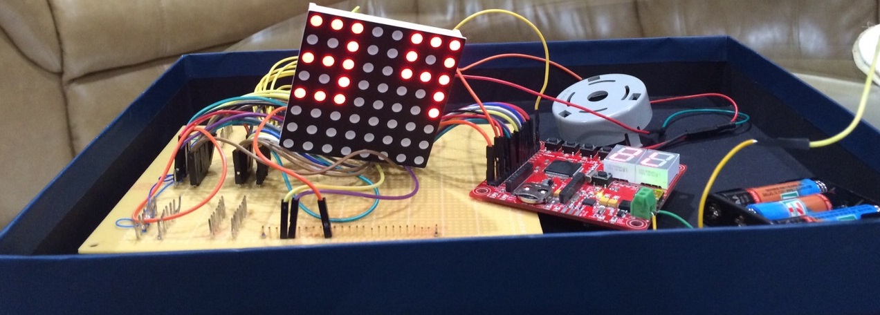
| − | [ | + | [[File:S15 146 G5 Final Project2.jpg|center]] |
== Abstract == | == Abstract == | ||
| Line 29: | Line 29: | ||
=== Team Members & Responsibilities === | === Team Members & Responsibilities === | ||
| − | + | #David Whiting: Programmer and Report Writer | |
| − | + | #Ann Varakukala: Programmer and Report Writer | |
| − | + | #Navleen Johal: Programmer and Report Writer | |
== Schedule == | == Schedule == | ||
| Line 145: | Line 145: | ||
== Design & Implementation == | == Design & Implementation == | ||
| − | |||
=== Hardware Design === | === Hardware Design === | ||
| Line 152: | Line 151: | ||
=== 8x8 RGB LED Board Matrix === | === 8x8 RGB LED Board Matrix === | ||
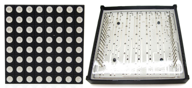
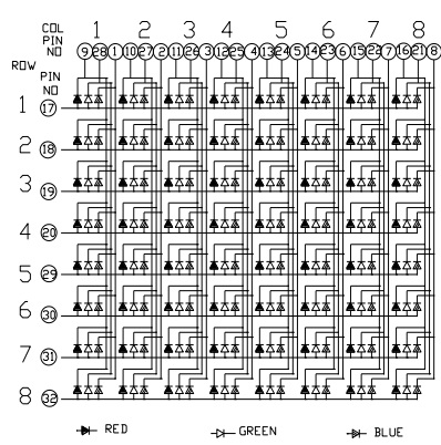
| − | The 8x8 RGB LED Board used for this project can be seen in Figure 1 and the schematics of this board can be seen in Figure 2 | + | The 8x8 RGB LED Board used for this project can be seen in Figure 1 and the schematics of this board can be seen in Figure 2. Using the schematics seen below, we were able to determine which pins needed to be selected to turn on or off a certain LED in the LED Matrix. For example, to turn on the Green LED on the first row and first column of the LED Board, pins 17 and 28 must be enabled. |
| + | This particular 8x8 LED Board contains 64 Red, 64 Green, and 64 Blue LEDs. Using all three colors, our goal is to display the current time, temperature, and allow the user to set the alarm time on this LED display. | ||
| − | Figure 1: 8x8 RGB LED Board | + | [[File:S15_146_G5_LED_front_and_back.png|center|frame|Figure 1: 8x8 RGB LED Board]] |
| − | Figure 2: 8x8 RGB LED Board Schematics | + | |
| + | [[File:S15_146_G5_LED_Schematic.jpg|center|frame|Figure 2: 8x8 RGB LED Board Schematics]] | ||
===Shift Register=== | ===Shift Register=== | ||
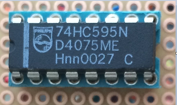
| − | The SN74HC595 Shift Register, is an 8-bit Shift Register that provides the micro controller with additional inputs or outputs. The | + | The SN74HC595 Shift Register, is an 8-bit Shift Register that provides the micro controller with additional inputs or outputs. The Shift Register used for this project can be seen in Figure 3. It can shift and hold the data that is inputted into the shift register. The outputs of the shift register are all in parallel and are used to turn the LEDs on and off. In this project, it provides a means for the micro controller to control the columns of the LED Matrix. As there are three different LED colors on the LED Board, it is necessary to add a total of three Shift Registers to the circuit, one for each color. The Shift Register has an output enable pin, which is used to enable and disable all the outputs of the register. When the data pin is High, then a 1 is pushed into the shift register, and when the data pin is Low, a 0 is pushed into the shift register. The Latch pin is enabled once all eight values are received, and is copied to the latch register, and is turns on the selected LEDs. |
| + | [[File:S15_146_G5_Shift_Register.png|center|frame|Figure 3: SN74HC595 Shift Register]] | ||
| − | Figure | + | ===PWM Buzzer=== |
| + | A Buzzer is used in this project to act as an alarm sound when the alarm time set by the user has been reached. Figure 4 depicts the buzzer that was used for this project. | ||
| + | [[File:S15_146_G5_Buzzer.jpg|center|frame|Figure 4: Buzzer]] | ||
| − | === | + | ===Power Supply=== |
| − | + | In order for the project to work without being connected to a computer, a battery pack holder containing 3 AAA batteries is used as the power supply. The power supply is used to power our entire circuit, and will allow this project to be more mobile. Figure 5 depicts the battery pack holder that was used for this project. | |
| + | |||
| + | |||
| + | [[File:S15_146_G5_Battery_Pack_Holder.png|center|frame|Figure 5: Battery Pack Holder]] | ||
| + | |||
| + | ===Accelerometer=== | ||
| + | The information taken from the on-board accelerometer is used to vary the hours and minutes for the alarm time. When the SJSUOne Board is tilted to the left, the user can decrease the hours or minutes, and when the SJSUOne Board is tilted to the right, the user is able to increase the hours or minutes. | ||
| + | ===Light Sensor=== | ||
| + | Due to the limitation of the size of the LED Matrix, it was necessary to split the time into two sections; the hours and minutes and display it at two separate times. This was done using the on-board Light Sensor. When the light source on the sensor is blocked, for example, a hand hovering over the sensor, the hour of the current time or the alarm time will be seen on the clock, while the current minutes or the alarm minutes disappear. When the hand is removed, thus letting light enter into the light sensor, the minutes is displayed on the LED Matrix. This hand gesture technique is just a special way to accommodate with the small LED Matrix screen. | ||
| − | |||
| + | ===Block Diagram of System=== | ||
| + | Figure 6 illustrates the block diagram of our entire system, which consists of one SJSUOne Board, a PWM Buzzer, one Shift Register, and one 8x8 RGB LED Board. | ||
| − | + | [[File:S15_146_G5_BlockDiagram1.jpg|center|frame|Figure 6: System Block Diagram]] | |
| − | |||
| − | Figure | + | ===System Schematics=== |
| + | Figure 7 illustrates the schematics of the entire system. In the end, we only used the red LEDs from the LED Board, and as a result, we only needed one shift register. | ||
| + | [[File:S15 146 G5 Schematics1.jpg|center|frame|Figure 7: System Schematics]] | ||
=== Hardware Interface === | === Hardware Interface === | ||
| − | In this section, | + | |
| + | In our project, our board communicates with the peripheral devices with three different methods. These three methods are SPI, PWM, and GPIO. Each of these different methods will be discussed below. | ||
| + | |||
| + | === SPI === | ||
| + | |||
| + | In our design, we used the pins P0.7 and P0.9 for the SCLK and MOSI respectively. Master out feeds into the shift registers so to allow the registers to output the desired data. The sclk from the SJSU One board feeds into both clock ports of the shift registers. Currently, the primary shift register output enable pin is connected to ground to permanently show the color red. The initialization code is shown below. | ||
| + | |||
| + | <pre> | ||
| + | void sck_initialize() | ||
| + | { | ||
| + | //step 1: Power on SPI | ||
| + | LPC_SC->PCONP |= (1 << 10); | ||
| + | //step 2: Set Clock | ||
| + | LPC_SC->PCLKSEL0 &= ~(3 << 20); //Clears bits 20 and 21 | ||
| + | LPC_SC->PCLKSEL0 |= (1 << 20); //Sets clock bits to 01 which set it to PCLK_peripheral = CCLK (On page 58 of User manual) | ||
| + | //It can be set with BIT(LPC_SC->PCLKSEL0).b21_20=1 but i prefer this way for learning purposes | ||
| + | //step 3: Select the SSP pins | ||
| + | LPC_GPIO0->FIODIR |= (1 << 6); | ||
| + | LPC_PINCON->PINSEL0 &= ~(3 << 14); | ||
| + | LPC_PINCON->PINSEL0 &= ~(3 << 16); | ||
| + | LPC_PINCON->PINSEL0 &= ~(3 << 18); | ||
| + | //This clears in order: SCK1, MOSI1, MISO1 (page 117) | ||
| + | LPC_PINCON->PINSEL0 |= (2 << 14); | ||
| + | LPC_PINCON->PINSEL0 |= (2 << 16); | ||
| + | LPC_PINCON->PINSEL0 |= (2 << 18); | ||
| + | //This sets in order: SCK1, MOSI1, MISO1 (page 117) | ||
| + | //This two lines could have been set with BIT(LPC_SC->PINSEL0).b commands | ||
| + | //step 4: Interrupts (Not done for this lab) | ||
| + | //~~~~~~~~~~~~~~~~~~~~~~~~~~~~~~~~~~~~~~~~~~~~~~~~~~~~~~~~~~~~~~~~~~~~~~~~~~~~~~~~~~~~~~~~~~~~~~~~~~~~~~~~~~~~ | ||
| + | //step 5: Initialization | ||
| + | LPC_SSP1->CR0 = 7; //This gives us 8 bit mode because 7=111 in binary. Same as (7<<0) | ||
| + | LPC_SSP1->CR1 = 2; //This sets bit 1 to 1 because 2=10_2. This allows the SSP controller to interact | ||
| + | //with other devices on the serial bus. Same as (1<<1) | ||
| + | LPC_SSP1->CPSR = 254; //This value was used because it was in the tutorial. It can however go down to 2. The range | ||
| + | //as specified by the user manual is 2 or larger (only even number page 433) | ||
| + | //The number specified acts as a divider for the clock so this means SCK=CPU/8 | ||
| + | |||
| + | } | ||
| + | </pre> | ||
| + | |||
| + | Once this is initialized data can then be sent with the function hex_commands(char command) This will be explored later in the software implementation section. | ||
| + | |||
| + | ===GPIO=== | ||
| + | |||
| + | To control the LEDs on the LED matrix, the column and the row of the LED matrix must both be activated to turn on the LED. The row operations are controlled by the GPIO pins on the board and the columns of the LED matrix are controlled by the shift register. A sample of code showing this in action can be seen below. | ||
| + | |||
| + | <pre> | ||
| + | ensure_byte(0x7F); | ||
| + | rowenable(8); | ||
| + | delay_ms(1); | ||
| + | rowdisable(8); | ||
| + | </pre> | ||
| + | The code above shows the process of how to display an object on the LED matrix. The code above was taken from the alarm display portion. | ||
| + | |||
| + | === Buzzer === | ||
| + | |||
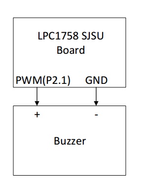
| + | The buzzer is used to sound off when the alarm has been activated. The alarm is connected to a pwm input on the SJSU One board, which can be seen in Figure 9. To sound the buzzer, a frequency and a set percentage needs to be set to allow the buzzer to turn on. A sample of this is shown in the code below. | ||
| + | |||
| + | [[File:S15 146 G5 Buzzer2.jpg|center|frame|Figure 9: Buzzer connected to SJSUOne Board]] | ||
| + | |||
| + | <pre> | ||
| + | PWM pwm(PWM::pwm2, 300); | ||
| + | pwm.set(50); | ||
| + | </pre> | ||
| + | |||
| + | The code above sets the buzzer to 300 Hz and sets the percentage to 50 percent. The percentage is for the duty cycle. With 50 percent duty cycle that means that the signal was active during 50 percent of the one off period. | ||
=== Software Design === | === Software Design === | ||
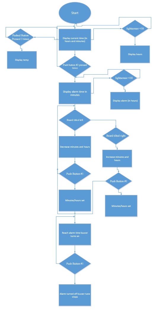
| − | + | When designing our project, it was necessary to create a flowchart that would help us meet all the objectives and help us identify how the program is to be controlled. In Figure 8, it depicts our Software Design Flow, going into detail of what are the steps if certain buttons are pressed and goes into detail of how the alarm time is set based on the board orientation. | |
| + | |||
| + | [[File:S15_146_G5_FlowChart.jpg|center|frame|Figure 8: Software Design Flow]] | ||
=== Implementation === | === Implementation === | ||
This section includes implementation, but again, not the details, just the high level. For example, you can list the steps it takes to communicate over a sensor, or the steps needed to write a page of memory onto SPI Flash. You can include sub-sections for each of your component implementation. | This section includes implementation, but again, not the details, just the high level. For example, you can list the steps it takes to communicate over a sensor, or the steps needed to write a page of memory onto SPI Flash. You can include sub-sections for each of your component implementation. | ||
| + | |||
| + | ===FreeRTOS=== | ||
| + | |||
| + | The foundation of all our software design was with the use of FreeRTOS. FreeRTOS allows us to run multiple queues and tasks to allow us to run all of our different operations seamlessly together.The different tasks that utilized FreeRTOS will be discussed later in this section. | ||
| + | |||
| + | === 8x8 LED Matrix === | ||
| + | |||
| + | The LED display is the most important part of the software design because it is our output display. The way that the LED Matrix display works is by breaking each character into two to three different steps, depending on the character. For example, if attempting to print the number three onto the LED display, the first step would be to display the three horizontal lines and then next display the vertical line on the right side of the number. To send the correct data to the shift registers, SPI communication is used. In some implementations, an extra chip is used to control the rows of the LED display, however this was not implemented and instead the GPIO pins on the SJSU One board. Excerpts of code from each of the previously mentioned designs will be shown below. | ||
| + | |||
| + | <pre> | ||
| + | |||
| + | char hex_commands(char command) | ||
| + | { | ||
| + | LPC_SSP1->DR = command; | ||
| + | while (LPC_SSP1->SR & (1 << 4)) | ||
| + | ; | ||
| + | return LPC_SSP1->DR; | ||
| + | } | ||
| + | |||
| + | </pre> | ||
| + | |||
| + | The above code was used to send the necessary data to our shift registers to output the correct data. The below code was used to display the number 3. Note for this design, all active signals are low. | ||
| + | |||
| + | <pre> | ||
| + | ensure_byte(0xF8); | ||
| + | rowenable(1); | ||
| + | rowenable(3); | ||
| + | rowenable(5); | ||
| + | |||
| + | delay_ms(1); | ||
| + | rowdisable(1); | ||
| + | rowdisable(3); | ||
| + | rowdisable(5); | ||
| + | ensure_byte(0xFB); | ||
| + | rowenable(2); | ||
| + | rowenable(4); | ||
| + | |||
| + | delay_ms(1); | ||
| + | rowdisable(2); | ||
| + | rowdisable(4); | ||
| + | </pre> | ||
| + | Lastly the code below is used to enable the rows when called. | ||
| + | <pre> | ||
| + | if (a != 8) | ||
| + | { | ||
| + | if (a == 1) | ||
| + | { | ||
| + | row = 19; | ||
| + | } | ||
| + | if (a == 2) | ||
| + | { | ||
| + | row = 20; | ||
| + | } | ||
| + | if (a == 3) | ||
| + | { | ||
| + | row = 22; | ||
| + | } | ||
| + | if (a == 4) | ||
| + | { | ||
| + | row = 23; | ||
| + | } | ||
| + | if (a == 5) | ||
| + | { | ||
| + | row = 28; | ||
| + | } | ||
| + | if (a == 6) | ||
| + | { | ||
| + | row = 29; | ||
| + | } | ||
| + | if (a == 7) | ||
| + | { | ||
| + | row = 31; | ||
| + | } | ||
| + | |||
| + | LPC_GPIO1->FIOSET = (1 << row); | ||
| + | } | ||
| + | |||
| + | else | ||
| + | { | ||
| + | LPC_GPIO0->FIOSET = (1 << 26); | ||
| + | } | ||
| + | </pre> | ||
| + | |||
| + | ==== Light Sensor ==== | ||
| + | |||
| + | The use of this sensors, as stated previously, is to be able to read both the hours and the minutes on the alarm clock. It is used by having the sensor constantly taking light readings, and when the readings get below a certain threshold, the hours will display instead of the default minutes. A portion of this code can be seen below. | ||
| + | <pre> | ||
| + | if (LS.getPercentValue()<10 &&visual==0) | ||
| + | </pre> | ||
| + | The code above checks the light coming in and if the percent light that the sensor is receiving is less than 10 percent, the board will display hours. | ||
| + | |||
| + | ===Acceleration Sensor=== | ||
| + | |||
| + | To be able to select the desired time and alarm time, the on-board acceleration sensor was used. The acceleration sensor calculated its position and incremented or decremented the desired time to according to which position it was facing. A portion of the code is shown below. | ||
| + | |||
| + | <pre> | ||
| + | if((AS.getX()>0&&AS.getY()>0) || (AS.getX()<0&&AS.getY()>0)) | ||
| + | { | ||
| + | |||
| + | // puts("\nRight\n"); | ||
| + | orientation_t orientation=right; | ||
| + | |||
| + | xQueueSend(getSharedObject(shared_SensorQueueId), &orientation, 1000); | ||
| + | |||
| + | } | ||
| + | |||
| + | |||
| + | if (right == orientation) | ||
| + | { | ||
| + | minute_1++; | ||
| + | |||
| + | // puts("\nTask 2 right\n"); | ||
| + | } | ||
| + | |||
| + | </pre> | ||
| + | |||
| + | As seen above, when the board recognizes that it is facing in the right direction, it puts its orientation into a queue and allows for another task to read and increment the time accordingly. | ||
| + | |||
| + | === Temperature Sensor === | ||
| + | |||
| + | The temperature sensor is used to calculate the temperature inside the users room. The temperature senor was set up by using the commands that were provided with the development kit. These functions can be found in io.hpp. Because our display works with one digit at a time, the temperature had to be divided up into its individual parts. This can be seen below. | ||
| + | |||
| + | <pre> | ||
| + | int div = 0, mod = 0, temp = TS.getFarenheit(); | ||
| + | |||
| + | div=temp/10; | ||
| + | mod=temp%10; | ||
| + | </pre> | ||
| + | |||
| + | ===Acceleration Sensor=== | ||
| + | |||
| + | To be able to select the desired time and alarm time, the on-board acceleration sensor was used. The acceleration sensor calculated its position and incremented or decremented the desired time to according to which position it was facing. A portion of the code is shown below. | ||
| + | |||
| + | <pre> | ||
| + | if((AS.getX()>0&&AS.getY()>0) || (AS.getX()<0&&AS.getY()>0)) | ||
| + | { | ||
| + | |||
| + | // puts("\nRight\n"); | ||
| + | orientation_t orientation=right; | ||
| + | |||
| + | xQueueSend(getSharedObject(shared_SensorQueueId), &orientation, 1000); | ||
| + | |||
| + | } | ||
| + | |||
| + | |||
| + | if (right == orientation) | ||
| + | { | ||
| + | minute_1++; | ||
| + | |||
| + | // puts("\nTask 2 right\n"); | ||
| + | } | ||
| + | |||
| + | </pre> | ||
| + | |||
| + | As seen above, when the board recognizes that it is facing in the right direction, it puts its orientation into a queue and allows for another task to read and increment the time accordingly. | ||
| + | |||
| + | === Temperature Sensor === | ||
| + | |||
| + | The temperature sensor is used to calculate the temperature inside the users room. The temperature senor was set up by using the commands that were provided with the development kit. These functions can be found in io.hpp. Because our display works with one digit at a time, the temperature had to be divided up into its individual parts. This can be seen below. | ||
| + | |||
| + | <pre> | ||
| + | int div = 0, mod = 0, temp = TS.getFarenheit(); | ||
| + | |||
| + | div=temp/10; | ||
| + | mod=temp%10; | ||
| + | </pre> | ||
== Testing & Technical Challenges == | == Testing & Technical Challenges == | ||
| Line 195: | Line 442: | ||
Include sub-sections that list out a problem and solution, such as: | Include sub-sections that list out a problem and solution, such as: | ||
| − | === | + | === Issue #1 === |
| − | The first issue that we encountered was getting the three different LED colors to light up on the board correctly and determine which pins controlled each row. The pins on the LED Board were not labelled, so we had to do trial and error to figure out which pins were which according to the schematics. While overcoming this problem, we gained a deeper understanding of how the board functions as well as inspiring us to implement the project in a more efficient manner. | + | The first issue that we encountered was getting the three different LED colors to light up on the board correctly and determine which pins controlled each row. The pins on the LED Board were not labelled as seen in Figure 1, so we had to do trial and error to figure out which pins were which according to the schematics. To avoid further confusion, we labelled the pins on the board. Labeling the different pins on the back of the board is highly recommended for anyone who is planning on working with this 8x8 RGB LED Board. While overcoming this problem, we gained a deeper understanding of how the board functions as well as inspiring us to implement the project in a more efficient manner. |
| − | === | + | === Issue #2 === |
| − | The second issue that we encountered was getting the numbers to output correctly on the screen | + | The second issue that we encountered was getting the numbers 0-9 to output correctly on the screen as our initial hex values for enabling the rows were not correct. When we tested the values on the board, we were able to determine why the numbers were not outputting correctly on the board. We realized that when we did the calculations for the hex values, we had the msb and the lsb in reverse. Once we recalculated and fixed all the hex values, we were able to successfully get the numbers 0-9, to output correctly on the board. |
| + | |||
| + | === Issue #3 === | ||
| + | After meeting all the objectives, we decided to implement the different colors to the board and give the user the option to select a color mode, which allows them to choose which color to display on the board. However, when we wired another two shift registers, one for the Blue LEDs and the other for the Green LEDs, we were getting various combinations of color, which was not what we are expecting. After much troubleshooting, we decided to stick a single color for the entire board. For future recommendations, we would recommend using a PCB design to eliminate a lot of the wiring, thus making troubleshooting a lot easier. | ||
| + | |||
| + | === Issue #4 === | ||
| + | When we implemented the PWM Buzzer to our project, we wanted to make a melodious tune rather than the single buzzer note. However, when we performed testing on the buzzer, we encountered a problem. We realized that our tune for the buzzer would only emit sound at certain alarm times or would emit the sound later at the set alarm time. We simplified the tune emitted from the buzzer and we were able to successfully have it emit sound for all alarm times. | ||
| − | |||
| − | |||
== Conclusion == | == Conclusion == | ||
| − | + | ||
| + | Overall, we were able to successfully meet all the objectives that were promised at the beginning of the semester. To make the process more smoother in terms of debugging, we would highly recommend future students consider making a PCB design to avoid possible wiring mistakes or wires being loose and save time debugging the circuit. Furthermore, we have gained a deeper understanding of how to create multiple FreeRTOS tasks, and how to use the on-board delays to create our very own clock. Moreover, we were able to incorporate various on-board sensors such as the light sensor, temperature sensor, and the accelerometer. | ||
=== Project Video === | === Project Video === | ||
| − | Below is a short video demonstrating our project. | + | Below is a link to a short video demonstrating the functionalities of our project. |
| + | |||
| + | https://www.youtube.com/watch?v=gAbxosA0ur4 | ||
=== Project Source Code === | === Project Source Code === | ||
| − | * [https://sourceforge.net/projects/ | + | * [https://sourceforge.net/projects/led-alarm-clock/files/?source=navbar Sourceforge Source Code Link] |
== References == | == References == | ||
Latest revision as of 05:41, 26 May 2015
Contents
- 1 Grading Criteria
- 2 Tilt Motion Controlled LED Alarm Clock
- 3 Abstract
- 4 Objectives & Introduction
- 5 Schedule
- 6 Parts List & Cost
- 7 Design & Implementation
- 7.1 Hardware Design
- 7.2 8x8 RGB LED Board Matrix
- 7.3 Shift Register
- 7.4 PWM Buzzer
- 7.5 Power Supply
- 7.6 Accelerometer
- 7.7 Light Sensor
- 7.8 Block Diagram of System
- 7.9 System Schematics
- 7.10 Hardware Interface
- 7.11 SPI
- 7.12 GPIO
- 7.13 Buzzer
- 7.14 Software Design
- 7.15 Implementation
- 7.16 FreeRTOS
- 7.17 8x8 LED Matrix
- 7.18 Acceleration Sensor
- 7.19 Temperature Sensor
- 7.20 Acceleration Sensor
- 7.21 Temperature Sensor
- 8 Testing & Technical Challenges
- 9 Conclusion
- 10 References
Grading Criteria
- How well is Software & Hardware Design described?
- How well can this report be used to reproduce this project?
- Code Quality
- Overall Report Quality:
- Software Block Diagrams
- Hardware Block Diagrams
- Schematic Quality
- Quality of technical challenges and solutions adopted.
Tilt Motion Controlled LED Alarm Clock
Abstract
The Tilt Motion Controlled LED Alarm Clock is system that will allow the user to set an alarm using the SJSUOne Board. Users can view the time on an 8X8 RBG LED Board, and can manipulate the hours and minutes by tilting the board left and right respectively. A buzzer will be used as alarm tone, when the alarm goes off.
Objectives & Introduction
This system will be utilizing the accelerometer on the SJSUOne Board to allow the user to tilt the board left and right to adjust timing for the alarm. An 8X8 RGB LED Board is used to display the time and the user can see the number change instantaneously. A buzzer will turn on to alert the user the inputted time has been reached.
The Objectives of this project:
- Research and design the schematics to connect and power the 8X8 LED Board to the SJSUOne Board
- Complete the hardware according to schematics
- Test LED Board and light up individual LEDs and use shift register to shift LEDs across the screen
- Display time and temperature on the LED board
- Program the SJSUOne Board to vary the alarm time using the on-board accelerometer
- Program a PWM buzzer to turn on when alarm time has been reached
Team Members & Responsibilities
- David Whiting: Programmer and Report Writer
- Ann Varakukala: Programmer and Report Writer
- Navleen Johal: Programmer and Report Writer
Schedule
| Week# | Start Date | End Date | Task | Actual |
|---|---|---|---|---|
| 1 | 4/6 | 4/12 | Continue to conduct research necessary for the project.
Understand the schematics of each part. Design the schematics for project. |
Parts were received and team members looked over the schematics of the necessary parts and designed the schematics for the project. |
| 2 | 4/13 | 4/19 | Build the schematics and check if the LEDs on the board light up.
Test to see if individual bits light up. Understand how to control the red, green, and blue LEDs on the board. |
Individual LEDs and rows of LEDs were lit up using a 5V Power Supply. Tested various connections to determine how to select certain colors and LEDs. |
| 3 | 4/20 | 4/26 | Continue to work on building the project by connecting to SJSUOne Board.
Program GPIO pins to control the rows on the 8X8 Led Board. |
LED Board has been successfully connected to the SJSUOne Board using the GPIO pins to control the 8 rows on the board. |
| 4 | 4/27 | 5/3 | Program to display time on board.
Program push buttons for setting hours and minutes, AM and PM |
Using the 8x8 LED Board schematics, we determined which LEDs needed to be turned on to display the different numbers, using the corresponding hex values. |
| 5 | 5/4 | 5/10 | Continue to program to display time.
Tilt SJ One Board to change hours and minutes for setting the alarm. Program the buzzer to turn on when alarm time is reached |
Programmed the LED Board to display the different numbers. Furthermore, we were able to program our own clock and display the current time on the board. |
| 6 | 5/11 | 5/17 | Add and program additional sensors. Begin testing. | Programmed the alarm clock and using the on-board accelerometer, we were able to change the alarm times using the information gathered from the accelerometer. |
| 7 | 5/18 | 5/24 | Final Testing and Debugging. Finalize the Project Report. | We made the final touches to both our hardware and software design, double checking that everything is 100% functional. We created an encasing for the project, to increase visual appeal and prevent wires from moving around. Furthermore, we updated our schematics to reflect the recent changes and completed the report. |
| 8 | 5/25 | 5/25 | Demo Day | We demoed our project to the CMPE 146 and 244 class. |
Parts List & Cost
| Quantity | Item | Cost |
|---|---|---|
| 1 | SJ One Board | $80.00 |
| 1 | 8X8 RGB LED Board | $7.50 |
| 3 | SN74HC595: Shift Register | $1.05 |
| 24 | 220 Ohm Resistors | $0.20 |
| 1 | Female to Female Jumper Wires | $6.00 |
| 1 | Buzzer | $0.55 |
| 1 | Battery Pack Holder | $0.75 |
| 3 | AAA Batteries | $4.99 |
Design & Implementation
Hardware Design
Discuss your hardware design here. Show detailed schematics, and the interface here. Below is a list of major components necessary for this project, followed by a detailed description of the schematics of the entire system.
8x8 RGB LED Board Matrix
The 8x8 RGB LED Board used for this project can be seen in Figure 1 and the schematics of this board can be seen in Figure 2. Using the schematics seen below, we were able to determine which pins needed to be selected to turn on or off a certain LED in the LED Matrix. For example, to turn on the Green LED on the first row and first column of the LED Board, pins 17 and 28 must be enabled.
This particular 8x8 LED Board contains 64 Red, 64 Green, and 64 Blue LEDs. Using all three colors, our goal is to display the current time, temperature, and allow the user to set the alarm time on this LED display.
Shift Register
The SN74HC595 Shift Register, is an 8-bit Shift Register that provides the micro controller with additional inputs or outputs. The Shift Register used for this project can be seen in Figure 3. It can shift and hold the data that is inputted into the shift register. The outputs of the shift register are all in parallel and are used to turn the LEDs on and off. In this project, it provides a means for the micro controller to control the columns of the LED Matrix. As there are three different LED colors on the LED Board, it is necessary to add a total of three Shift Registers to the circuit, one for each color. The Shift Register has an output enable pin, which is used to enable and disable all the outputs of the register. When the data pin is High, then a 1 is pushed into the shift register, and when the data pin is Low, a 0 is pushed into the shift register. The Latch pin is enabled once all eight values are received, and is copied to the latch register, and is turns on the selected LEDs.
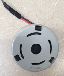
PWM Buzzer
A Buzzer is used in this project to act as an alarm sound when the alarm time set by the user has been reached. Figure 4 depicts the buzzer that was used for this project.
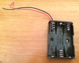
Power Supply
In order for the project to work without being connected to a computer, a battery pack holder containing 3 AAA batteries is used as the power supply. The power supply is used to power our entire circuit, and will allow this project to be more mobile. Figure 5 depicts the battery pack holder that was used for this project.
Accelerometer
The information taken from the on-board accelerometer is used to vary the hours and minutes for the alarm time. When the SJSUOne Board is tilted to the left, the user can decrease the hours or minutes, and when the SJSUOne Board is tilted to the right, the user is able to increase the hours or minutes.
Light Sensor
Due to the limitation of the size of the LED Matrix, it was necessary to split the time into two sections; the hours and minutes and display it at two separate times. This was done using the on-board Light Sensor. When the light source on the sensor is blocked, for example, a hand hovering over the sensor, the hour of the current time or the alarm time will be seen on the clock, while the current minutes or the alarm minutes disappear. When the hand is removed, thus letting light enter into the light sensor, the minutes is displayed on the LED Matrix. This hand gesture technique is just a special way to accommodate with the small LED Matrix screen.
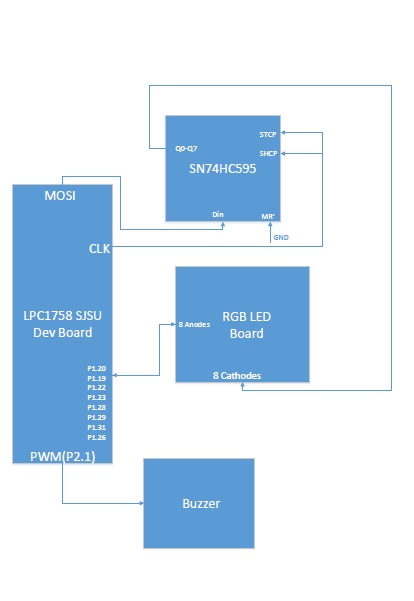
Block Diagram of System
Figure 6 illustrates the block diagram of our entire system, which consists of one SJSUOne Board, a PWM Buzzer, one Shift Register, and one 8x8 RGB LED Board.
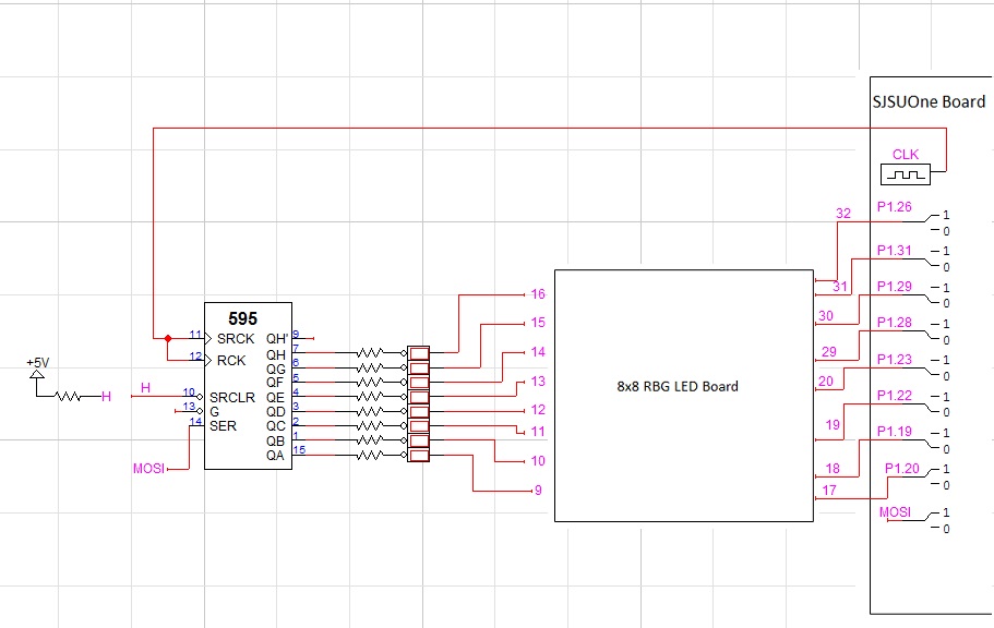
System Schematics
Figure 7 illustrates the schematics of the entire system. In the end, we only used the red LEDs from the LED Board, and as a result, we only needed one shift register.
Hardware Interface
In our project, our board communicates with the peripheral devices with three different methods. These three methods are SPI, PWM, and GPIO. Each of these different methods will be discussed below.
SPI
In our design, we used the pins P0.7 and P0.9 for the SCLK and MOSI respectively. Master out feeds into the shift registers so to allow the registers to output the desired data. The sclk from the SJSU One board feeds into both clock ports of the shift registers. Currently, the primary shift register output enable pin is connected to ground to permanently show the color red. The initialization code is shown below.
void sck_initialize()
{
    //step 1:  Power on SPI
    LPC_SC->PCONP |= (1 << 10);
    //step 2:  Set Clock
    LPC_SC->PCLKSEL0 &= ~(3 << 20); //Clears bits 20 and 21
    LPC_SC->PCLKSEL0 |= (1 << 20); //Sets clock bits to 01 which set it to PCLK_peripheral = CCLK (On page 58 of User manual)
                                   //It can be set with BIT(LPC_SC->PCLKSEL0).b21_20=1 but i prefer this way for learning purposes
    //step 3:  Select the SSP pins
    LPC_GPIO0->FIODIR |= (1 << 6);
    LPC_PINCON->PINSEL0 &= ~(3 << 14);
    LPC_PINCON->PINSEL0 &= ~(3 << 16);
    LPC_PINCON->PINSEL0 &= ~(3 << 18);
//This clears in order:  SCK1, MOSI1, MISO1 (page 117)
    LPC_PINCON->PINSEL0 |= (2 << 14);
    LPC_PINCON->PINSEL0 |= (2 << 16);
    LPC_PINCON->PINSEL0 |= (2 << 18);
//This sets in order:  SCK1, MOSI1, MISO1 (page 117)
//This two lines could have been set with BIT(LPC_SC->PINSEL0).b commands
    //step 4:  Interrupts (Not done for this lab)
//~~~~~~~~~~~~~~~~~~~~~~~~~~~~~~~~~~~~~~~~~~~~~~~~~~~~~~~~~~~~~~~~~~~~~~~~~~~~~~~~~~~~~~~~~~~~~~~~~~~~~~~~~~~~
    //step 5:  Initialization
    LPC_SSP1->CR0 = 7; //This gives us 8 bit mode because 7=111 in binary.  Same as (7<<0)
    LPC_SSP1->CR1 = 2; //This sets bit 1 to 1 because 2=10_2.  This allows the SSP controller to interact
                       //with other devices on the serial bus.  Same as (1<<1)
    LPC_SSP1->CPSR = 254; //This value was used because it was in the tutorial.  It can however go down to 2.  The range
                          //as specified by the user manual is 2 or larger (only even number page 433)
                          //The number specified acts as a divider for the clock so this means SCK=CPU/8

}
Once this is initialized data can then be sent with the function hex_commands(char command) This will be explored later in the software implementation section.
GPIO
To control the LEDs on the LED matrix, the column and the row of the LED matrix must both be activated to turn on the LED. The row operations are controlled by the GPIO pins on the board and the columns of the LED matrix are controlled by the shift register. A sample of code showing this in action can be seen below.
ensure_byte(0x7F);
rowenable(8);
delay_ms(1);
rowdisable(8);
The code above shows the process of how to display an object on the LED matrix. The code above was taken from the alarm display portion.
Buzzer
The buzzer is used to sound off when the alarm has been activated. The alarm is connected to a pwm input on the SJSU One board, which can be seen in Figure 9. To sound the buzzer, a frequency and a set percentage needs to be set to allow the buzzer to turn on. A sample of this is shown in the code below.
 PWM pwm(PWM::pwm2, 300);
 pwm.set(50);
The code above sets the buzzer to 300 Hz and sets the percentage to 50 percent. The percentage is for the duty cycle. With 50 percent duty cycle that means that the signal was active during 50 percent of the one off period.
Software Design
When designing our project, it was necessary to create a flowchart that would help us meet all the objectives and help us identify how the program is to be controlled. In Figure 8, it depicts our Software Design Flow, going into detail of what are the steps if certain buttons are pressed and goes into detail of how the alarm time is set based on the board orientation.
Implementation
This section includes implementation, but again, not the details, just the high level. For example, you can list the steps it takes to communicate over a sensor, or the steps needed to write a page of memory onto SPI Flash. You can include sub-sections for each of your component implementation.
FreeRTOS
The foundation of all our software design was with the use of FreeRTOS. FreeRTOS allows us to run multiple queues and tasks to allow us to run all of our different operations seamlessly together.The different tasks that utilized FreeRTOS will be discussed later in this section.
8x8 LED Matrix
The LED display is the most important part of the software design because it is our output display. The way that the LED Matrix display works is by breaking each character into two to three different steps, depending on the character. For example, if attempting to print the number three onto the LED display, the first step would be to display the three horizontal lines and then next display the vertical line on the right side of the number. To send the correct data to the shift registers, SPI communication is used. In some implementations, an extra chip is used to control the rows of the LED display, however this was not implemented and instead the GPIO pins on the SJSU One board. Excerpts of code from each of the previously mentioned designs will be shown below.
char hex_commands(char command)
{
    LPC_SSP1->DR = command;
    while (LPC_SSP1->SR & (1 << 4))
        ;
    return LPC_SSP1->DR;
}
The above code was used to send the necessary data to our shift registers to output the correct data. The below code was used to display the number 3. Note for this design, all active signals are low.
ensure_byte(0xF8);
rowenable(1);
rowenable(3);
rowenable(5);

delay_ms(1);
rowdisable(1);
rowdisable(3);
rowdisable(5);
ensure_byte(0xFB);
rowenable(2);
rowenable(4);

delay_ms(1);
rowdisable(2);
rowdisable(4);
Lastly the code below is used to enable the rows when called.
 if (a != 8)
    {
        if (a == 1)
        {
            row = 19;
        }
        if (a == 2)
        {
            row = 20;
        }
        if (a == 3)
        {
            row = 22;
        }
        if (a == 4)
        {
            row = 23;
        }
        if (a == 5)
        {
            row = 28;
        }
        if (a == 6)
        {
            row = 29;
        }
        if (a == 7)
        {
            row = 31;
        }

        LPC_GPIO1->FIOSET = (1 << row);
    }

    else
    {
        LPC_GPIO0->FIOSET = (1 << 26);
    }
Light Sensor
The use of this sensors, as stated previously, is to be able to read both the hours and the minutes on the alarm clock. It is used by having the sensor constantly taking light readings, and when the readings get below a certain threshold, the hours will display instead of the default minutes. A portion of this code can be seen below.
if (LS.getPercentValue()<10 &&visual==0)
The code above checks the light coming in and if the percent light that the sensor is receiving is less than 10 percent, the board will display hours.
Acceleration Sensor
To be able to select the desired time and alarm time, the on-board acceleration sensor was used. The acceleration sensor calculated its position and incremented or decremented the desired time to according to which position it was facing. A portion of the code is shown below.
 if((AS.getX()>0&&AS.getY()>0) || (AS.getX()<0&&AS.getY()>0))
                 {

                     // puts("\nRight\n");
                      orientation_t orientation=right;

                      xQueueSend(getSharedObject(shared_SensorQueueId), &orientation, 1000);

                 }


if (right == orientation)
                {
                    minute_1++;

                    // puts("\nTask 2 right\n");
                }
As seen above, when the board recognizes that it is facing in the right direction, it puts its orientation into a queue and allows for another task to read and increment the time accordingly.
Temperature Sensor
The temperature sensor is used to calculate the temperature inside the users room. The temperature senor was set up by using the commands that were provided with the development kit. These functions can be found in io.hpp. Because our display works with one digit at a time, the temperature had to be divided up into its individual parts. This can be seen below.
int div = 0, mod = 0, temp = TS.getFarenheit();

                div=temp/10;
                mod=temp%10;
Testing & Technical Challenges
Describe the challenges of your project. What advise would you give yourself or someone else if your project can be started from scratch again? Make a smooth transition to testing section and described what it took to test your project.
Include sub-sections that list out a problem and solution, such as:
Issue #1
The first issue that we encountered was getting the three different LED colors to light up on the board correctly and determine which pins controlled each row. The pins on the LED Board were not labelled as seen in Figure 1, so we had to do trial and error to figure out which pins were which according to the schematics. To avoid further confusion, we labelled the pins on the board. Labeling the different pins on the back of the board is highly recommended for anyone who is planning on working with this 8x8 RGB LED Board. While overcoming this problem, we gained a deeper understanding of how the board functions as well as inspiring us to implement the project in a more efficient manner.
Issue #2
The second issue that we encountered was getting the numbers 0-9 to output correctly on the screen as our initial hex values for enabling the rows were not correct. When we tested the values on the board, we were able to determine why the numbers were not outputting correctly on the board. We realized that when we did the calculations for the hex values, we had the msb and the lsb in reverse. Once we recalculated and fixed all the hex values, we were able to successfully get the numbers 0-9, to output correctly on the board.
Issue #3
After meeting all the objectives, we decided to implement the different colors to the board and give the user the option to select a color mode, which allows them to choose which color to display on the board. However, when we wired another two shift registers, one for the Blue LEDs and the other for the Green LEDs, we were getting various combinations of color, which was not what we are expecting. After much troubleshooting, we decided to stick a single color for the entire board. For future recommendations, we would recommend using a PCB design to eliminate a lot of the wiring, thus making troubleshooting a lot easier.
Issue #4
When we implemented the PWM Buzzer to our project, we wanted to make a melodious tune rather than the single buzzer note. However, when we performed testing on the buzzer, we encountered a problem. We realized that our tune for the buzzer would only emit sound at certain alarm times or would emit the sound later at the set alarm time. We simplified the tune emitted from the buzzer and we were able to successfully have it emit sound for all alarm times.
Conclusion
Overall, we were able to successfully meet all the objectives that were promised at the beginning of the semester. To make the process more smoother in terms of debugging, we would highly recommend future students consider making a PCB design to avoid possible wiring mistakes or wires being loose and save time debugging the circuit. Furthermore, we have gained a deeper understanding of how to create multiple FreeRTOS tasks, and how to use the on-board delays to create our very own clock. Moreover, we were able to incorporate various on-board sensors such as the light sensor, temperature sensor, and the accelerometer.
Project Video
Below is a link to a short video demonstrating the functionalities of our project.
https://www.youtube.com/watch?v=gAbxosA0ur4
Project Source Code
References
Acknowledgement
- Dr. Haluk Özemek
- Preetpal Kang
References Used
List any references used in project.
[1] 8x8 RGB LED Matrix Schematics: http://www.vetco.net/datasheets/VUPN6866/GTM2088ARGB-21.pdf
[2] SN74HC595 Shift Register Schematics: http://www.ti.com/lit/ds/symlink/sn74hc595.pdf
[3] FreeRTOS Tasks Lab Assignment: http://www.socialledge.com/sjsu/index.php?title=Embedded_System_Tutorial_FreeRTOS
[4] PWM Buzzer: http://www.socialledge.com/sjsu/index.php?title=SJ_One_Board
Appendix
You can list the references you used.
